A 4-layer PCB offers enhanced signal integrity, reduced electromagnetic interference, and better power distribution compared to a 2-layer PCB, making it ideal for complex and high-speed circuits. Explore the rest of the article to understand which PCB type best suits Your electronic project needs.
Comparison Table
| Feature | 4-Layer PCB | 2-Layer PCB |
|---|---|---|
| Layer Count | 4 layers (2 signal, 2 power/ground) | 2 layers (top and bottom signal layers) |
| Signal Integrity | Better signal integrity and reduced EMI | Moderate signal integrity, higher EMI |
| Complexity | Supports complex circuit designs | Suitable for simpler circuits |
| Board Size | Smaller board footprint for same circuit | Larger board size for complex circuits |
| Manufacturing Cost | Higher due to more layers | Lower cost, simpler manufacturing |
| Thermal Management | Improved heat dissipation | Limited heat dissipation |
| Applications | High-speed, high-density electronics | Basic consumer electronics |
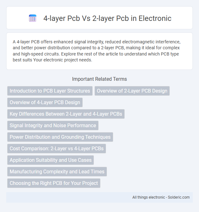
Introduction to PCB Layer Structures
A 4-layer PCB features two additional internal layers compared to a 2-layer PCB, enhancing signal integrity, power distribution, and electromagnetic interference (EMI) reduction. The extra layers in a 4-layer PCB allow for dedicated ground and power planes, improving overall circuit performance and reliability. Understanding the differences in layer structures helps you select the right PCB type for complex, high-speed, or high-density electronic designs.
Overview of 2-Layer PCB Design
2-layer PCB design involves two conductive copper layers separated by an insulating substrate, typically providing a simple yet effective solution for moderate circuit complexity and cost-efficiency. These PCBs balance signal integrity and manufacturing ease, supporting through-hole and surface-mount components while offering improved routing capabilities compared to single-layer designs. Ideal for applications requiring moderate electrical performance, 2-layer PCBs are widely used in consumer electronics, automotive systems, and industrial controls where compactness and reliability are essential.
Overview of 4-Layer PCB Design
4-layer PCBs consist of four conductive layers, typically arranged with two signal layers separated by two internal planes for power and ground, enhancing electrical performance and reducing electromagnetic interference. This multilayer structure allows for more complex circuit designs and better signal integrity compared to 2-layer PCBs, which only have two signal layers on opposite sides. The additional layers in 4-layer PCBs support improved routing density, efficient power distribution, and thermal management, making them ideal for high-frequency and high-speed applications.
Key Differences Between 2-Layer and 4-Layer PCBs
A 4-layer PCB offers enhanced signal integrity and reduced electromagnetic interference compared to a 2-layer PCB by incorporating additional internal power and ground planes. This structure supports higher circuit density, improved thermal management, and better noise reduction, making it ideal for complex designs. In contrast, 2-layer PCBs are simpler, cost-effective for basic applications but limited in handling high-speed signals and complex routing requirements.
Signal Integrity and Noise Performance
A 4-layer PCB offers superior signal integrity and noise performance compared to a 2-layer PCB due to its dedicated ground and power planes that reduce electromagnetic interference and crosstalk. The additional layers provide controlled impedance pathways, minimizing signal reflection and attenuation, which is critical for high-speed and high-frequency applications. Your design will benefit from enhanced signal quality and improved noise immunity with a 4-layer PCB, especially in complex or sensitive electronic circuits.
Power Distribution and Grounding Techniques
A 4-layer PCB offers dedicated power and ground planes that significantly improve signal integrity and reduce electromagnetic interference compared to 2-layer PCBs, where power and ground traces share layers with signals. The solid power and ground planes in 4-layer designs provide lower impedance paths, better current handling, and enhanced noise isolation, critical for high-speed or sensitive circuits. In contrast, 2-layer PCBs rely on less efficient power distribution and grounding methods, often resulting in increased crosstalk and voltage drops.
Cost Comparison: 2-Layer vs 4-Layer PCBs
2-layer PCBs generally offer lower manufacturing costs due to simpler fabrication processes and less material usage, making them ideal for budget-sensitive projects. In contrast, 4-layer PCBs incur higher expenses because of additional layers requiring more complex lamination, drilling, and quality control steps. Despite the increased cost, 4-layer PCBs provide enhanced electrical performance and design flexibility, often justifying the investment in more advanced applications.
Application Suitability and Use Cases
4-layer PCBs offer enhanced signal integrity and reduced electromagnetic interference, making them suitable for complex applications like high-speed communication devices, RF circuits, and advanced computing systems. 2-layer PCBs are typically used in simpler, cost-sensitive applications such as consumer electronics, automotive controls, and basic power supplies where design complexity and signal interference are minimal. The choice between 4-layer and 2-layer PCBs depends on the required electrical performance, space constraints, and budget considerations specific to the end-use scenario.
Manufacturing Complexity and Lead Times
A 4-layer PCB involves more intricate manufacturing processes than a 2-layer PCB due to additional layering, requiring precise alignment and lamination steps that extend production time. This complexity often results in longer lead times and increased costs as specialized equipment and quality control measures are necessary to ensure reliability. Your project timelines should account for these factors when choosing between 2-layer and 4-layer PCB options to balance performance needs with manufacturing efficiency.
Choosing the Right PCB for Your Project
Choosing the right PCB for your project depends on complexity, signal integrity, and budget constraints. A 4-layer PCB offers improved electromagnetic interference (EMI) reduction, superior power distribution, and better signal routing for high-speed circuits, making it ideal for complex designs requiring reliability. In contrast, a 2-layer PCB is cost-effective and suitable for simpler projects with less stringent electrical performance needs.
4-layer pcb vs 2-layer pcb Infographic