A PIN diode offers excellent high-frequency switching and low distortion in RF applications due to its intrinsic layer, whereas a resistance switching diode primarily functions by changing resistance states for memory and sensing uses. Explore the rest of the article to understand which diode best suits your electronic design needs.
Comparison Table
| Feature | PIN Diode | Resistance Switching Diode |
|---|---|---|
| Structure | Intrinsic layer between P and N regions | Specialized material with resistance change properties |
| Function | RF switch, variable resistor in high-frequency circuits | Switches resistance states for memory and switching |
| Switching Speed | Moderate to high speed switching | Fast switching based on resistance change |
| Applications | RF attenuation, phase shifters, signal modulation | Non-volatile memory, resistive RAM, programmable devices |
| Power Handling | High power RF signals | Low power electronic switching |
| Control | Bias current controls conductivity | Voltage or current induces resistance state change |
| Latency | Nanoseconds to microseconds | Nanoseconds to milliseconds depending on material |
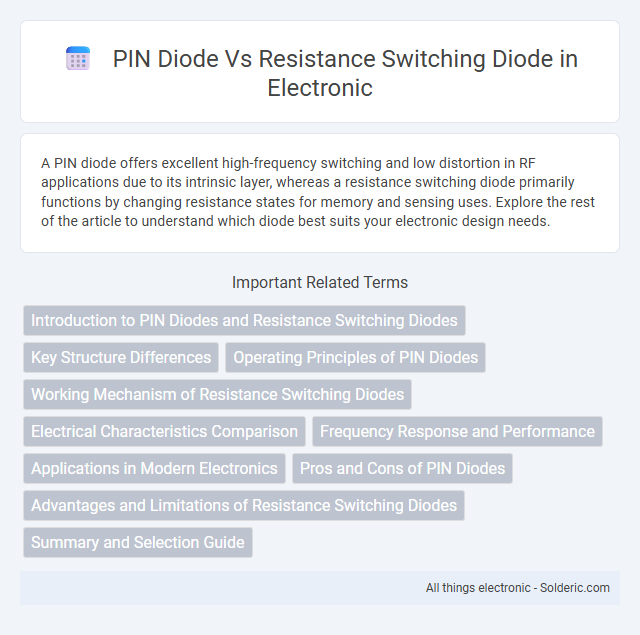
Introduction to PIN Diodes and Resistance Switching Diodes
PIN diodes feature an intrinsic layer between the p-type and n-type regions, enabling efficient radio frequency (RF) switching and attenuation by controlling charge storage in the depletion region. Resistance switching diodes operate by altering their resistance state under applied voltage, commonly used in memory devices and neuromorphic computing applications. Your choice between PIN and resistance switching diodes depends on requirements like high-frequency performance for RF circuits or non-volatile resistance changes for digital storage.
Key Structure Differences
PIN diodes feature an intrinsic (undoped) layer sandwiched between the p-type and n-type regions, enhancing their ability to handle high-frequency signals and power applications by providing controlled conductivity. Resistance switching diodes lack this intrinsic layer, relying instead on changes in the material's resistance to switch states, typically enabling faster switching speeds but with limited power handling capability. The presence of the intrinsic layer in PIN diodes results in larger depletion regions, making them suitable for RF attenuation and switching, whereas resistance switching diodes prioritize quick resistive state changes for memory and logic applications.
Operating Principles of PIN Diodes
PIN diodes operate by creating an intrinsic layer between the p-type and n-type regions, allowing control of RF signals through changes in carrier injection and depletion. Resistance switching diodes function by altering their resistance state via an applied voltage that induces filament formation or rupture in the switching material. The fundamental difference lies in the PIN diode's use of charge carrier modulation, while resistance switching diodes rely on resistive state transitions for signal modulation.
Working Mechanism of Resistance Switching Diodes
Resistance switching diodes operate based on reversible changes in their resistance states, caused by the formation and rupture of conductive filaments within the device's active layer under an applied voltage. This memristive behavior enables the diode to switch between high resistance (OFF) and low resistance (ON) states without relying on the charge storage mechanism typical in PIN diodes. Unlike PIN diodes that modulate conductivity through carrier injection and recombination in the intrinsic layer, resistance switching diodes utilize physical structural changes at the nanoscale to achieve non-volatile memory and switching functions.
Electrical Characteristics Comparison
PIN diodes exhibit low capacitance and high switching speed due to their intrinsic layer, making them ideal for high-frequency applications, while resistance switching diodes typically have higher resistance states and slower switching times. The forward voltage drop of a PIN diode is generally lower than that of a resistance switching diode, which affects signal attenuation and efficiency in RF circuits. Your choice depends on whether you prioritize low insertion loss and fast response (PIN diode) or simple resistance state control for memory and logic applications (resistance switching diode).
Frequency Response and Performance
PIN diodes exhibit superior frequency response compared to resistance switching diodes due to their intrinsic layer, which reduces junction capacitance and enables faster switching speeds in RF and microwave applications. Resistance switching diodes often suffer from slower response times and higher signal loss, making them less suitable for high-frequency performance. Your choice should prioritize PIN diodes when optimal frequency response and reliable performance in high-speed circuits are critical.
Applications in Modern Electronics
PIN diodes excel in RF switching and attenuator circuits due to their low capacitance and fast switching speeds, making them ideal for high-frequency applications like radar and wireless communication systems. Resistance switching diodes, characterized by their ability to toggle between high and low resistance states, are pivotal in memory storage devices and reconfigurable logic circuits within modern electronics. Both diode types enable efficient control of current flow, but their distinct electrical properties cater to specialized roles across telecommunications, signal processing, and advanced computing technologies.
Pros and Cons of PIN Diodes
PIN diodes offer fast switching speeds, high linearity, and low distortion, making them ideal for RF and microwave applications, but they suffer from higher cost and lower power handling compared to resistance switching diodes. Their intrinsic layer provides excellent isolation and low capacitance in the off state, enhancing performance in attenuators and switches, whereas resistance switching diodes have simpler structures with faster switching but less precision. The main trade-off for PIN diodes lies in balancing their superior frequency response against increased complexity and potential thermal management challenges.
Advantages and Limitations of Resistance Switching Diodes
Resistance switching diodes offer advantages such as faster switching speeds and lower power consumption compared to PIN diodes, making them suitable for high-frequency and low-power applications. Their compact size and simpler fabrication processes contribute to cost-effectiveness and integration in miniaturized circuits. However, resistance switching diodes face limitations including lower power handling capability and reduced linearity, which can affect performance in high-power and precision signal applications.
Summary and Selection Guide
PIN diodes offer excellent RF switching capabilities due to their low forward resistance and high isolation, making them ideal for high-frequency applications like attenuators and phase shifters. Resistance switching diodes, which function by altering resistance states, are better suited for low-frequency or digital switching tasks where fast state change and simple control are required. Your choice depends on application frequency, switching speed, and insertion loss requirements, with PIN diodes favored for microwave frequencies and resistance switching diodes suited for cost-effective, low-frequency solutions.
PIN diode vs resistance switching diode Infographic