Flip-chip technology offers superior electrical performance and thermal management by directly attaching the die to the substrate, reducing signal path lengths compared to wire bonding. Discover how understanding these differences can optimize your electronic device design by reading the full article.
Comparison Table
| Feature | Flip-Chip | Wire Bond |
|---|---|---|
| Interconnection Method | Solder bumps directly connect chip to substrate | Fine metal wires connect chip pads to package leads |
| Electrical Performance | Lower inductance and resistance, better signal integrity | Higher inductance, suitable for lower frequency |
| Thermal Dissipation | Superior thermal conduction through the substrate | Less efficient heat dissipation |
| Package Size | More compact, reduced footprint | Larger due to wire loops |
| Manufacturing Complexity | Higher complexity, requires advanced equipment | Lower complexity, widely used standard |
| Cost | Generally higher due to equipment and materials | Lower, cost-effective for mass production |
| Reliability | Better mechanical strength, less susceptible to vibration | Wires prone to breakage in harsh conditions |
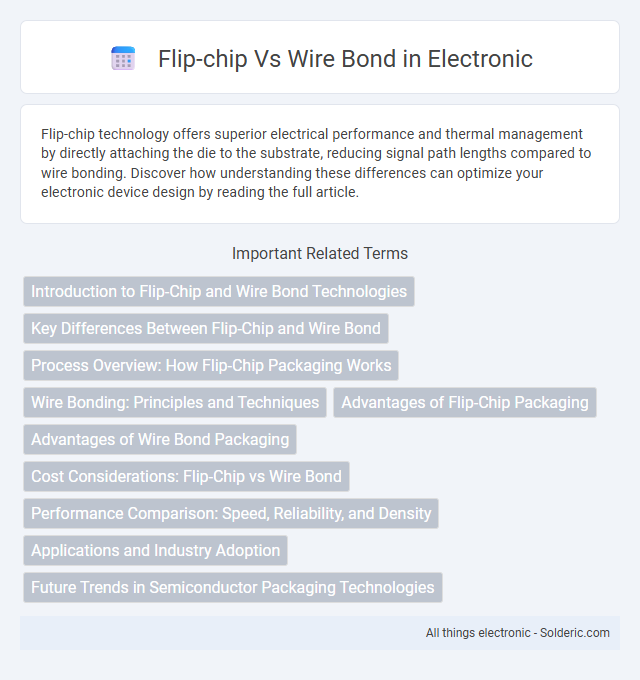
Introduction to Flip-Chip and Wire Bond Technologies
Flip-chip technology involves directly mounting the semiconductor die onto the substrate using solder bumps, offering improved electrical performance and heat dissipation compared to wire bond methods. Wire bonding connects the die to the package leads using fine metal wires, a traditional technique known for its simplicity and cost-effectiveness. Your choice between flip-chip and wire bond depends on factors like device complexity, performance requirements, and manufacturing costs.
Key Differences Between Flip-Chip and Wire Bond
Flip-chip technology features direct electrical connections through solder bumps on the chip's surface, providing shorter interconnects and superior electrical performance compared to wire bonding's use of thin wires to connect the chip to the package. Flip-chip supports higher input/output (I/O) density and enhanced thermal dissipation, while wire bond is typically simpler, more cost-effective, and better suited for low to moderate I/O counts. The main distinctions lie in packaging complexity, electrical performance, thermal management, and scalability for advanced semiconductor applications.
Process Overview: How Flip-Chip Packaging Works
Flip-chip packaging involves directly attaching the semiconductor die to the substrate using solder bumps that replace traditional wire bonds, enabling shorter electrical paths and improved performance. During the process, solder bumps are deposited on the die's pads, flipped, and aligned precisely with matching pads on the substrate before reflow soldering secures the connection. This method enhances thermal dissipation and electrical efficiency, offering a compact and reliable alternative to conventional wire bonding techniques.
Wire Bonding: Principles and Techniques
Wire bonding, a fundamental semiconductor packaging technique, involves creating electrical interconnections by bonding fine wires from the chip's pads to the package leads using ultrasonic, thermosonic, or thermocompression methods. Gold, aluminum, and copper are common bonding materials chosen based on electrical performance and mechanical reliability requirements. Your device's performance and manufacturing efficiency depend significantly on precise control of wire bonding parameters and optimization of materials used.
Advantages of Flip-Chip Packaging
Flip-chip packaging offers significant advantages such as reduced parasitic inductance and resistance, enabling faster signal transmission and improved electrical performance. This packaging method provides a smaller footprint and enhanced thermal dissipation, which supports higher power densities and reliability in compact electronic devices. You benefit from these features through improved device efficiency, miniaturization, and greater overall system performance compared to traditional wire bonding.
Advantages of Wire Bond Packaging
Wire bond packaging offers superior flexibility in connecting multiple die types and sizes, making it ideal for complex multi-chip modules. The process allows for reliable electrical connections with lower manufacturing costs compared to flip-chip technology. Enhanced thermal performance and ease of repair or rework further increase the practicality of wire bond solutions in various semiconductor applications.
Cost Considerations: Flip-Chip vs Wire Bond
Flip-chip technology typically incurs higher initial costs due to complex fabrication and alignment processes, making it more expensive than wire bonding for low to medium volume production. Wire bond offers a cost-effective solution with simpler manufacturing and established tooling, ideal for high-volume, less complex designs. However, flip-chip's superior electrical performance and miniaturization benefits can justify its higher expense in advanced applications requiring high speed and density.
Performance Comparison: Speed, Reliability, and Density
Flip-chip technology offers superior speed due to shorter interconnect paths, reducing signal delay and enhancing high-frequency performance compared to wire bond methods. Reliability is improved in flip-chip designs since solder bumps provide robust mechanical and thermal connections, minimizing failure risks common in wire bonds caused by wire fatigue and breakage. Your device benefits from higher density with flip-chip packaging, enabling more I/O connections and compact layouts than wire bonding, which is limited by wire spacing constraints.
Applications and Industry Adoption
Flip-chip technology is widely adopted in high-performance computing, smartphones, and automotive electronics due to its superior electrical and thermal performance. Wire bond remains prevalent in cost-sensitive applications such as consumer electronics, medical devices, and power modules because of its simplicity and reliability. Semiconductor manufacturers increasingly favor flip-chip for advanced packaging in AI accelerators and 5G infrastructure, while wire bond continues to serve established markets with mature production ecosystems.
Future Trends in Semiconductor Packaging Technologies
Flip-chip technology is gaining momentum due to its superior electrical performance, higher input/output density, and better thermal management compared to traditional wire bond methods. Advanced packaging trends emphasize heterogeneous integration and 3D stacking, where flip-chip enables shorter interconnects and enhanced signal integrity critical for AI and 5G applications. Emerging innovations such as fan-out wafer-level packaging (FO-WLP) and embedded bridge technology further enhance the flip-chip approach, positioning it as the future standard in high-performance semiconductor packaging.
Flip-chip vs Wire bond Infographic