Floating-gate technology stores charge on a conductive floating gate, enabling reliable data retention and faster programming in non-volatile memory devices, while charge-trap memory uses an insulating layer to trap electrons, offering simpler fabrication and improved scalability. Explore the rest of the article to discover which memory type suits your needs best.
Comparison Table
| Feature | Floating-Gate | Charge-Trap |
|---|---|---|
| Storage Mechanism | Electrons stored on a conductive floating gate | Electrons trapped in a dielectric layer (charge-trap layer) |
| Technology Type | Traditional flash memory technology | Advanced flash memory technology (e.g., SONOS, TANOS) |
| Scalability | Limited by charge leakage and floating gate size | Better scalability due to thin dielectric layers |
| Program/Erase Speed | Moderate speed | Faster program and erase cycles |
| Endurance | Lower endurance due to oxide degradation | Higher endurance, less oxide stress |
| Data Retention | Reliable over 10+ years | Good retention, can be slightly less than floating-gate |
| Manufacturing Complexity | Established processes, mature technology | Requires advanced manufacturing, newer process |
| Use Cases | Legacy NAND flash, traditional EEPROMs | 3D NAND, embedded flash memory |
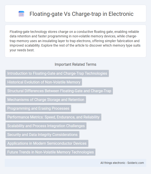
Introduction to Floating-Gate and Charge-Trap Technologies
Floating-gate and charge-trap technologies are two advanced memory storage methods used in non-volatile memory devices. Floating-gate technology stores electrical charge on an isolated conductive gate embedded within the transistor, enabling long-term data retention ideal for flash memory. Charge-trap technology, on the other hand, stores charge in an insulating layer, offering better scalability and resistance to charge leakage, which enhances device reliability and endurance for your storage needs.
Historical Evolution of Non-Volatile Memory
Floating-gate technology, pioneered in the 1960s, revolutionized non-volatile memory by allowing electrons to be stored on an insulated gate, enabling data retention without power. Charge-trap memory emerged later, utilizing silicon nitride layers to trap charges, offering improved scaling, endurance, and simpler manufacturing processes. Your device's performance and longevity can benefit from understanding how these two technologies evolved to address the demands of modern data storage applications.
Structural Differences Between Floating-Gate and Charge-Trap
Floating-gate memory cells feature a conductive floating gate entirely surrounded by insulating oxide layers, which traps electrons to store charge. Charge-trap memory, by contrast, uses a dielectric layer embedded with localized charge-trapping sites, such as silicon nitride, instead of a continuous floating gate. This structural difference allows charge-trap devices to offer improved scalability and reduced interference between cells compared to floating-gate architectures.
Mechanisms of Charge Storage and Retention
Floating-gate memory stores charge within a conductive polysilicon layer completely insulated by oxide, enabling long data retention by trapping electrons in a well-defined quantum well. Charge-trap memory, however, retains charge in localized defect sites within a dielectric layer, often an oxide-nitride-oxide (ONO) stack, which offers enhanced scalability but can exhibit faster leakage due to trap-assisted tunneling. Your choice between these technologies should consider floating-gate's strong charge retention for stable, long-term storage versus charge-trap's potential for higher density and simplified fabrication.
Programming and Erasing Processes
Floating-gate memory programs by injecting electrons into the floating gate through Fowler-Nordheim tunneling or hot electron injection, while erasing involves removing these electrons via tunneling mechanisms, enabling precise charge control. Charge-trap memory stores charge in a dielectric layer with traps, programming by capturing electrons in localized states and erasing through charge detrapping or tunneling, often allowing faster and lower voltage operations. The differences in charge storage layers lead to distinct programming speeds, retention characteristics, and endurance, impacting device selection for specific non-volatile memory applications.
Performance Metrics: Speed, Endurance, and Reliability
Floating-gate memory cells exhibit faster programming and erasing speeds due to direct tunneling of electrons through a thin oxide barrier, while charge-trap devices rely on trapping charge in a dielectric layer, typically causing slower operation. In terms of endurance, charge-trap memories generally demonstrate superior cycle durability, often exceeding 10^6 program/erase cycles, compared to floating-gate cells whose oxide degradation limits their longevity. Reliability favors charge-trap memory with improved resistance to charge loss and better data retention over extended periods, as the discrete trapping sites reduce leakage pathways compared to the continuous floating-gate structure.
Scalability and Process Integration Challenges
Floating-gate technology faces scalability challenges due to charge leakage and limited oxide thickness reduction, which hinders further miniaturization in advanced nodes. Charge-trap memory offers better scalability by using a silicon nitride layer to trap charges, enabling thinner gate oxides and improved retention at smaller geometries. Despite improved scalability, charge-trap devices introduce complex process integration challenges such as precise control of trapping layer uniformity and reliability under high-voltage stress.
Security and Data Integrity Considerations
Floating-gate memory offers strong data retention and proven resistance to charge leakage, making it reliable for long-term security applications. Charge-trap technology provides enhanced endurance and better resistance to program/erase cycling stress, improving data integrity under frequent access conditions. Both architectures incorporate error-correction codes (ECC) and encryption methods to safeguard against data corruption and unauthorized access, with floating-gate often favored for secure firmware storage while charge-trap is preferred in advanced multi-level cell (MLC) memory solutions.
Applications in Modern Semiconductor Devices
Floating-gate technology is widely used in NAND flash memory, providing high endurance and reliable data storage for SSDs and USB drives. Charge-trap technology excels in embedded non-volatile memory applications, such as embedded flash in microcontrollers and system-on-chip (SoC) devices, due to its scalability and simpler fabrication process. Your choice of memory type may depend on the specific performance, density, and endurance requirements in modern semiconductor applications.
Future Trends in Non-Volatile Memory Technologies
Floating-gate technology, dominant in traditional NAND flash, faces scaling challenges due to cell-to-cell interference and charge leakage, prompting a shift towards charge-trap memory for improved endurance and scalability. Charge-trap memory, utilizing silicon nitride layers to store charges, offers better resistance to short-channel effects and allows for thinner oxide layers, positioning it as a strong candidate for 3D NAND architectures in future non-volatile memory development. Emerging trends emphasize integrating charge-trap structures with advanced process nodes and 3D stacking to enhance storage density, speed, and energy efficiency in next-generation non-volatile memory devices.
Floating-gate vs Charge-trap Infographic