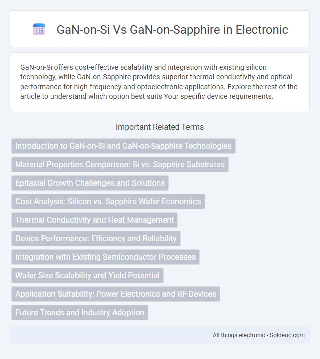
GaN-on-Si offers cost-effective scalability and integration with existing silicon technology, while GaN-on-Sapphire provides superior thermal conductivity and optical performance for high-frequency and optoelectronic applications. Explore the rest of the article to understand which option best suits Your specific device requirements.
Comparison Table
| Feature | GaN-on-Si | GaN-on-Sapphire |
|---|---|---|
| Substrate Material | Silicon (Si) | Sapphire (Al2O3) |
| Cost | Lower, due to silicon wafer availability | Higher, sapphire is more expensive |
| Thermal Conductivity | Moderate (~150 W/m*K) | Lower (~25 W/m*K) |
| Device Performance | Good, suitable for power electronics | Excellent for RF and optoelectronics |
| Integration | Compatible with CMOS processes | Less compatible with silicon CMOS |
| Defect Density | Higher threading dislocation density | Lower threading dislocation density |
| Wafer Size | Up to 200-300 mm | Limited to 100-150 mm |
| Applications | Power converters, LEDs, RF amplifiers | LEDs, lasers, RF devices, sensors |
Introduction to GaN-on-Si and GaN-on-Sapphire Technologies
GaN-on-Si technology integrates gallium nitride layers on silicon substrates, offering cost-effective manufacturing and larger wafer sizes beneficial for power electronics and RF applications. GaN-on-Sapphire uses sapphire substrates providing superior crystalline quality and high electron mobility ideal for high-frequency optoelectronic devices and LEDs. Choosing between GaN-on-Si and GaN-on-Sapphire depends on balancing substrate cost, thermal conductivity, and device performance requirements.
Material Properties Comparison: Si vs. Sapphire Substrates
GaN-on-Si substrates offer cost-effective manufacturing with excellent thermal conductivity (150 W/m*K) compared to sapphire's lower thermal conductivity (~35 W/m*K), enabling better heat dissipation in high-power applications. Silicon's larger wafer sizes (up to 300 mm) facilitate higher volume production than sapphire, which is limited to smaller diameters, improving scalability and reducing costs for GaN device fabrication. However, sapphire's superior electrical insulation and chemical stability support high-frequency and optoelectronic device performance, despite its higher expense and lower thermal management efficiency compared to Si substrates.
Epitaxial Growth Challenges and Solutions
GaN-on-Si faces epitaxial growth challenges such as lattice mismatch and thermal expansion differences that can cause dislocations and cracking, while GaN-on-Sapphire offers better lattice compatibility, resulting in fewer defects. Advanced buffer layers and strain management techniques mitigate these issues for GaN-on-Si, enhancing crystal quality and device performance. Your choice between these substrates impacts the complexity of epitaxial growth and overall semiconductor efficiency.
Cost Analysis: Silicon vs. Sapphire Wafer Economics
GaN-on-Si technology offers significant cost advantages over GaN-on-Sapphire due to the lower price and larger wafer sizes of silicon substrates, which enable higher throughput and reduced material expenses. Silicon wafers benefit from mature fabrication infrastructure, driving down processing costs, whereas sapphire wafers are more expensive and limited in size, impacting scalability and yield. Cost efficiency in GaN-on-Si makes it preferable for high-volume applications in power electronics and RF devices compared to the premium-priced GaN-on-Sapphire.
Thermal Conductivity and Heat Management
GaN-on-Si substrates offer superior thermal conductivity compared to GaN-on-Sapphire, enabling more efficient heat dissipation in high-power electronic devices. This enhanced heat management reduces thermal resistance, improving device reliability and performance under demanding operating conditions. Your choice of GaN-on-Si can significantly optimize thermal handling, leading to better thermal stability and longer device lifespan.
Device Performance: Efficiency and Reliability
GaN-on-Si devices offer higher thermal conductivity and cost-effective scalability, improving efficiency in power electronics compared to GaN-on-Sapphire. GaN-on-Sapphire provides superior electron mobility and reduced lattice mismatch, enhancing device reliability in RF applications. Reliability in GaN-on-Si is increasingly competitive, though GaN-on-Sapphire remains preferred where maximum performance and stability are critical.
Integration with Existing Semiconductor Processes
GaN-on-Si offers superior integration with existing semiconductor manufacturing processes due to the compatibility of silicon substrates with standard CMOS technology, allowing easier adoption in high-volume production. In contrast, GaN-on-Sapphire substrates require specialized processing techniques that limit seamless integration with traditional silicon-based fabs. The thermal expansion and lattice mismatch advantages of GaN-on-Si enable better scalability and cost-efficiency in mainstream semiconductor device fabrication.
Wafer Size Scalability and Yield Potential
GaN-on-Si offers superior wafer size scalability compared to GaN-on-Sapphire, enabling larger diameters up to 200 mm or more, which significantly reduces production costs and increases throughput. The yield potential for GaN-on-Si is generally higher due to better lattice matching and thermal expansion compatibility with silicon substrates, minimizing defects and wafer bowing. In contrast, GaN-on-Sapphire typically faces limitations in wafer size scalability, usually capped around 150 mm, and experiences lower yields due to higher dislocation densities and thermal mismatch stresses.
Application Suitability: Power Electronics and RF Devices
GaN-on-Si substrates excel in cost-effective power electronics applications due to their compatibility with existing silicon manufacturing infrastructure, offering high electron mobility and thermal conductivity suitable for high-voltage switching devices. In contrast, GaN-on-Sapphire substrates provide superior performance for RF devices, particularly in microwave and millimeter-wave frequencies, owing to their excellent insulating properties and high-frequency signal integrity. The choice between GaN-on-Si and GaN-on-Sapphire hinges on balancing cost-efficiency and thermal management in power electronics against low dielectric losses and high-frequency operation requirements in RF applications.
Future Trends and Industry Adoption
GaN-on-Si technology is rapidly gaining traction due to its cost-effectiveness and compatibility with existing silicon manufacturing infrastructure, making it a preferred choice for high-volume applications in power electronics and RF devices. GaN-on-Sapphire remains dominant in high-frequency and optoelectronic sectors like LEDs and RF amplifiers, benefiting from superior thermal performance and lattice matching. Your decision between these materials should factor in evolving industry standards, with GaN-on-Si expected to drive mainstream adoption as production scales and performance gaps narrow.
GaN-on-Si vs GaN-on-Sapphire Infographic