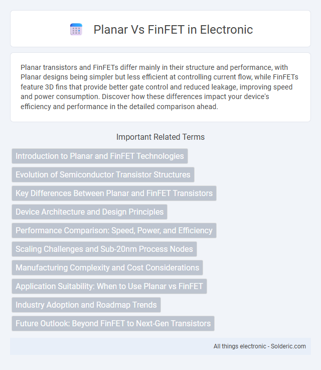
Planar transistors and FinFETs differ mainly in their structure and performance, with Planar designs being simpler but less efficient at controlling current flow, while FinFETs feature 3D fins that provide better gate control and reduced leakage, improving speed and power consumption. Discover how these differences impact your device's efficiency and performance in the detailed comparison ahead.
Comparison Table
| Feature | Planar Transistor | FinFET Transistor |
|---|---|---|
| Structure | Flat, 2D channel | 3D fin-shaped channel |
| Gate Control | Single gate | Multiple gates (3-sided control) |
| Leakage Current | Higher leakage due to weak gate control | Lower leakage with strong electrostatic control |
| Scaling Limit | Limited below 22nm nodes | Effective at 14nm and beyond |
| Performance | Lower drive current and speed | Higher drive current and improved speed |
| Power Efficiency | Less efficient, higher power consumption | More efficient, reduced power use |
| Manufacturing Complexity | Relatively simpler process | More complex fabrication process |
| Use Case | Older technology nodes, legacy designs | Advanced nodes, modern CPUs, GPUs |
Introduction to Planar and FinFET Technologies
Planar technology, used in traditional semiconductor devices, features flat, two-dimensional transistor structures that have been the foundation of integrated circuits for decades. FinFET technology introduces a three-dimensional, fin-shaped structure that enhances control over the channel, reducing leakage current and improving performance at smaller nodes. Your choice between Planar and FinFET impacts device efficiency, power consumption, and scalability for advanced electronics.
Evolution of Semiconductor Transistor Structures
Semiconductor transistor structures evolved from planar to FinFET designs to address scaling challenges and improve performance metrics such as leakage current and short-channel effects. Planar transistors feature a flat channel region, limiting electrostatic control as device dimensions shrink below 20nm, leading to increased power dissipation. FinFETs introduce a three-dimensional fin-shaped channel that surrounds the gate on multiple sides, enhancing gate control, reducing leakage, and enabling continued transistor scaling in advanced technology nodes like 7nm and 5nm.
Key Differences Between Planar and FinFET Transistors
Planar transistors feature a flat, two-dimensional channel for current flow, while FinFET transistors use a three-dimensional fin-shaped structure that wraps the gate around the channel, enhancing control over the current. FinFETs significantly reduce leakage current and improve performance at smaller technology nodes compared to planar designs, making them ideal for advanced, low-power semiconductor devices. Your choice between Planar and FinFET impacts device efficiency, scalability, and power consumption in integrated circuit design.
Device Architecture and Design Principles
Planar transistors feature a flat, two-dimensional channel where current flows horizontally beneath the gate, relying on traditional lithography for scaling and exhibiting limited control over short-channel effects. FinFET devices utilize a three-dimensional fin-shaped channel that wraps the gate on multiple sides, significantly enhancing electrostatic control and reducing leakage currents in advanced technology nodes. Your choice between Planar and FinFET architectures impacts power efficiency and transistor density due to their fundamentally different design principles and scalability advantages.
Performance Comparison: Speed, Power, and Efficiency
FinFET technology outperforms planar transistors in speed due to its 3D structure, which provides better control over current flow, minimizing leakage and enhancing switching performance. Your device benefits from lower power consumption and improved efficiency with FinFETs, as reduced short-channel effects decrease leakage currents and enable operation at lower voltages. This results in faster processing speeds and longer battery life compared to traditional planar transistors.
Scaling Challenges and Sub-20nm Process Nodes
Planar transistors face significant scaling challenges below 20nm process nodes due to short-channel effects and increased leakage currents, limiting performance and power efficiency. FinFET technology offers superior electrostatic control with its 3D structure, enabling better scaling and reduced leakage in sub-20nm nodes. Your designs benefit from FinFET's enhanced gate control, allowing continued advancement in transistor density and device performance at advanced manufacturing nodes.
Manufacturing Complexity and Cost Considerations
Planar transistors feature simpler manufacturing processes with established techniques, resulting in lower production costs compared to FinFETs. FinFET technology requires intricate 3D patterning and advanced lithography, increasing fabrication complexity and capital expenditure. Despite higher costs, FinFETs offer superior performance and power efficiency, justifying the investment for advanced semiconductor nodes.
Application Suitability: When to Use Planar vs FinFET
Planar transistors remain suitable for low-power, cost-sensitive applications such as microcontrollers and analog circuits where simplicity and proven design offer advantages. FinFET technology excels in high-performance computing, mobile processors, and AI accelerators due to superior control over short-channel effects and reduced leakage currents. Your choice depends on balancing power efficiency, process complexity, and performance requirements in the target application.
Industry Adoption and Roadmap Trends
FinFET technology has become the dominant semiconductor architecture in advanced nodes below 14nm, with major foundries like TSMC, Samsung, and Intel widely adopting it due to its superior performance, power efficiency, and scalability compared to planar transistors. Planar transistors continue to be used in mature process nodes above 14nm, mainly for cost-sensitive applications and legacy device manufacturing. Roadmap trends indicate a gradual phase-out of planar technology as industry focus shifts towards further FinFET enhancements and emerging architectures such as Gate-All-Around (GAA) transistors for nodes beyond 3nm.
Future Outlook: Beyond FinFET to Next-Gen Transistors
Next-generation transistors aim to surpass FinFET limitations by enhancing scalability, power efficiency, and performance for emerging technologies like AI and 5G. Innovations such as Gate-All-Around (GAA) and nanosheet transistors offer better electrostatic control and reduced leakage currents, enabling transistor nodes beyond 3nm. Semiconductor leaders like TSMC and Samsung are aggressively investing in these advanced architectures to maintain Moore's Law progression and meet the demands of future computing workloads.
Planar vs FinFET Infographic