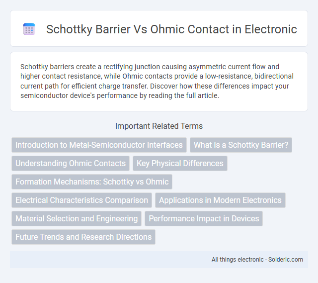
Schottky barriers create a rectifying junction causing asymmetric current flow and higher contact resistance, while Ohmic contacts provide a low-resistance, bidirectional current path for efficient charge transfer. Discover how these differences impact your semiconductor device's performance by reading the full article.
Comparison Table
| Feature | Schottky Barrier | Ohmic Contact |
|---|---|---|
| Contact Type | Rectifying (diode-like) | Non-rectifying (ohmic) |
| Current Flow | Unidirectional (limited by barrier) | Bidirectional, linear |
| Energy Barrier | Large Schottky barrier (~0.3 - 0.8 eV) | No significant barrier |
| Metal-Semiconductor Junction | Metal and semiconductor Fermi levels form barrier | Low resistance, metal facilitates carrier injection |
| Application | Schottky diodes, detectors, high-speed switching | Electrical contacts in devices, low-resistance paths |
| Resistance | High contact resistance | Low contact resistance |
| Carrier Transport Mechanism | Thermionic emission or tunneling over barrier | Ohmic conduction via tunneling or diffusion |
| Examples | Pt-Si, Au-GaAs | Al-Si, Ti-Au on n-type Si |
Introduction to Metal-Semiconductor Interfaces
Metal-semiconductor interfaces play a crucial role in electronic devices by controlling current flow between the metal electrode and semiconductor material. Schottky barriers form when there is a significant energy barrier at the metal-semiconductor junction, resulting in rectifying behavior with unidirectional current flow. In contrast, Ohmic contacts provide low-resistance, bidirectional current flow by minimizing the barrier height through metal selection or interface engineering, essential for efficient carrier injection in semiconductor devices.
What is a Schottky Barrier?
A Schottky barrier is a metal-semiconductor junction that forms a rectifying contact, allowing current to flow more easily in one direction than the other due to the built-in potential barrier at the interface. This barrier height depends on the metal work function and the semiconductor electron affinity, affecting charge carrier injection and device performance. Understanding the Schottky barrier is essential for optimizing your electronic devices, especially in applications requiring fast switching and low forward voltage drop.
Understanding Ohmic Contacts
Ohmic contacts provide a low-resistance electrical connection between a metal and a semiconductor, enabling efficient current flow without rectification. Unlike Schottky barriers, which create a potential energy barrier and exhibit diode-like behavior, ohmic contacts ensure linear current-voltage characteristics crucial for device performance. Your semiconductor devices rely on properly engineered ohmic contacts to minimize energy loss and maximize electrical conductivity.
Key Physical Differences
Schottky barriers exhibit a rectifying behavior due to the formation of a potential energy barrier at the metal-semiconductor interface, which restricts charge carrier flow based on barrier height and semiconductor doping level. Ohmic contacts provide a low-resistance, non-rectifying interface by enabling easy charge carrier injection through heavy doping or interface engineering, minimizing the barrier for current flow. Understanding these key physical differences helps optimize device performance depending on whether rectification or efficient charge conduction is required in your electronic application.
Formation Mechanisms: Schottky vs Ohmic
Schottky barrier formation occurs when a metal contacts a semiconductor, creating a potential energy barrier due to differences in work function and semiconductor electron affinity, which impedes carrier flow. Ohmic contact forms by heavily doping the semiconductor near the interface or using specific metals to bend the energy bands, allowing electrons to flow freely without significant resistance. Your device performance depends on choosing the appropriate contact type to ensure efficient charge injection or extraction for the intended application.
Electrical Characteristics Comparison
Schottky barriers exhibit rectifying behavior with a distinct potential barrier that causes nonlinear current-voltage (I-V) characteristics, resulting in a low forward voltage drop but limited reverse current flow. Ohmic contacts provide linear, low-resistance I-V characteristics, enabling efficient bidirectional current flow without significant voltage drop, essential for minimizing power loss in electronic devices. Your choice between Schottky barrier and Ohmic contact depends on whether rectification or low-resistance conduction is paramount for your semiconductor application.
Applications in Modern Electronics
Schottky barriers are essential in high-speed switching devices and RF applications due to their low forward voltage drop and fast switching characteristics. Ohmic contacts provide reliable, low-resistance connections in semiconductor devices, crucial for efficient current injection in transistors and integrated circuits. Both are integral to modern electronics, with Schottky barriers optimizing performance in detectors and power rectifiers, while Ohmic contacts ensure stable electrical connectivity in microprocessors and LED technology.
Material Selection and Engineering
Material selection for Schottky barriers typically involves metals with high work functions like platinum or gold to create a rectifying junction with semiconductors such as silicon or GaAs, optimizing electron barrier height and minimizing leakage currents. Ohmic contacts demand metals like aluminum or titanium that form low-resistance, non-rectifying interfaces through heavily doped semiconductor regions, ensuring efficient charge carrier injection. Engineering techniques like surface cleaning, interface passivation, and controlled annealing tailor the contact properties by influencing interfacial states and metal diffusion, directly impacting device performance and reliability.
Performance Impact in Devices
Schottky barriers create a rectifying junction that significantly influences device performance by introducing a built-in potential barrier, which affects current flow and switching speed in diodes and transistors. Ohmic contacts provide low-resistance, linear current-voltage characteristics essential for efficient charge injection and extraction, resulting in minimal power loss and improved device efficiency. The choice between Schottky and Ohmic contacts directly impacts device behavior, reliability, and the overall performance of semiconductor components such as field-effect transistors (FETs) and photovoltaic cells.
Future Trends and Research Directions
Emerging research focuses on engineering Schottky barriers with tunable barrier heights to optimize electron transport in next-generation electronic devices, including high-speed transistors and sensors. Advanced materials like 2D semiconductors and novel metal alloys are being explored to create low-resistance Ohmic contacts that minimize energy loss and enhance device efficiency. Future trends emphasize integrating machine learning for contact interface design, aimed at achieving reliable, scalable manufacturing of both Schottky and Ohmic contacts in flexible and nanoelectronics applications.
Schottky barrier vs Ohmic contact Infographic