Triple-well processes offer enhanced isolation for sensitive circuits compared to twin-well architectures, improving noise immunity and reducing latch-up risks in mixed-signal designs. Explore the rest of the article to understand how these well structures impact your semiconductor device performance and design choices.
Comparison Table
| Feature | Triple-well | Twin-well |
|---|---|---|
| Definition | Semiconductor structure with three wells: p-well, deep n-well, and n-well | Semiconductor structure with two wells: p-well and n-well |
| Isolation | Enhanced isolation due to deep n-well for substrate noise reduction | Standard isolation between p-well and n-well |
| Use Case | High-performance mixed-signal ICs needing substrate noise immunity | General CMOS logic and analog circuits |
| Fabrication Complexity | Higher complexity and cost due to extra deep n-well implantation | Lower complexity and cost |
| Substrate Noise Immunity | Superior substrate noise isolation | Moderate substrate noise isolation |
| Power Consumption | Potentially higher due to larger well structures | Typically lower power consumption |
| Design Flexibility | Greater flexibility for mixed-signal integration | Standard flexibility suitable for most CMOS designs |
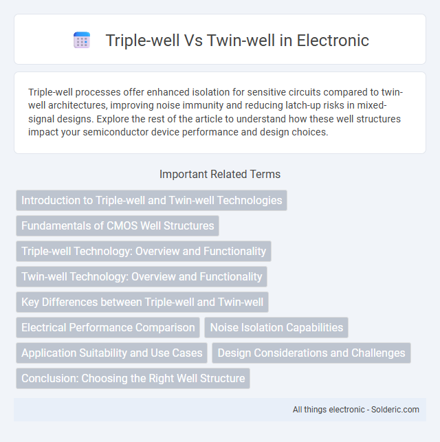
Introduction to Triple-well and Twin-well Technologies
Triple-well and twin-well technologies are advanced semiconductor fabrication techniques used to isolate transistors and reduce substrate noise in integrated circuits. Twin-well technology employs separate wells for NMOS and PMOS transistors, improving device performance by optimizing doping concentrations. Triple-well technology adds a buried well beneath the PMOS well, enhancing substrate isolation and enabling better control of transistor characteristics in high-performance analog and mixed-signal applications.
Fundamentals of CMOS Well Structures
Triple-well CMOS well structures incorporate an additional deep n-well that isolates the p-well from the substrate, enhancing latch-up immunity and reducing substrate noise coupling compared to twin-well designs. In twin-well processes, separate p-wells and n-wells are formed directly in the substrate, which can limit the control over body biasing and isolation effectiveness. The triple-well structure provides better isolation and flexibility in body bias control, making it suitable for mixed-signal and high-performance CMOS applications.
Triple-well Technology: Overview and Functionality
Triple-well technology enhances semiconductor device isolation by incorporating an additional well layer within the substrate, enabling improved control over parasitic capacitance and latch-up susceptibility compared to twin-well designs. This advanced structure allows precise voltage biasing of each well, optimizing device performance and reducing interference in integrated circuits. Understanding triple-well functionality can help you design more robust and efficient CMOS components for high-performance applications.
Twin-well Technology: Overview and Functionality
Twin-well technology uses separate p-type and n-type wells to isolate PMOS and NMOS transistors, improving device isolation and reducing latch-up susceptibility in CMOS integrated circuits. The p-well is embedded in an n-type substrate, while the n-well is diffused in a p-type substrate, allowing optimized threshold voltage control and enhanced transistor performance. This approach facilitates better noise margin and lower power consumption compared to single-well processes, making it suitable for mixed-signal and digital applications.
Key Differences between Triple-well and Twin-well
Triple-well technology features three distinct wells--one p-well sandwiched between two n-wells--offering superior isolation and reduced substrate noise compared to the twin-well structure, which consists of separate p-well and n-well regions. The enhanced isolation in triple-well processes enables better latch-up immunity and improved analog/digital integration on a single chip. Twin-well designs are simpler and cost-effective but may suffer from higher substrate coupling and limited flexibility in mixed-signal applications.
Electrical Performance Comparison
Triple-well technology offers superior electrical isolation by incorporating a deep n-well that surrounds p-wells, reducing latch-up susceptibility and minimizing substrate noise, resulting in enhanced electrical performance compared to twin-well structures. Twin-well devices are more prone to parasitic transistor activation and higher substrate coupling, which can degrade signal integrity and increase power consumption. Evaluating your circuit requirements, triple-well configurations provide better noise immunity and voltage threshold stability essential for high-performance and mixed-signal IC applications.
Noise Isolation Capabilities
Triple-well technology offers superior noise isolation capabilities compared to twin-well by incorporating an additional deep well structure that significantly reduces substrate coupling and minimizes electrical noise interference. The triple-well process effectively isolates sensitive analog and digital circuit components, enhancing signal integrity in mixed-signal integrated circuits. Improved noise immunity in triple-well designs results in better overall device performance, especially in high-frequency and low-noise applications.
Application Suitability and Use Cases
Triple-well technology offers enhanced isolation for mixed-signal and RF circuits, making it ideal for applications requiring high noise immunity and reduced substrate coupling, such as advanced analog-to-digital converters and sensitive sensor interfaces. Twin-well processes are better suited for standard CMOS digital circuits where moderate isolation and cost-effectiveness are prioritized, commonly found in microprocessors and memory devices. Your design choice depends on the need for isolation complexity versus overall process simplicity and cost efficiency.
Design Considerations and Challenges
Triple-well design incorporates an additional deep well compared to twin-well, enabling better isolation of NMOS transistors from substrate noise, crucial for mixed-signal ICs and RF applications. Twin-well processes simplify fabrication and reduce cost but present challenges in minimizing latch-up and substrate coupling, impacting overall device performance. Design considerations for triple-well focus on managing well-to-well capacitance and ensuring precise well-depth control to optimize noise isolation without significantly increasing area or process complexity.
Conclusion: Choosing the Right Well Structure
Triple-well structures offer enhanced isolation and reduced latch-up sensitivity, making them ideal for complex analog and mixed-signal circuits. Twin-well processes provide a balance of cost-efficiency and device performance suitable for standard CMOS digital applications. Selecting the right well structure depends on specific design requirements such as noise immunity, device density, and fabrication complexity.
Triple-well vs Twin-well Infographic