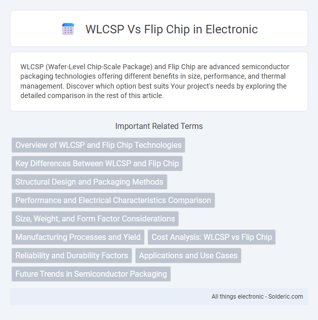
WLCSP (Wafer-Level Chip-Scale Package) and Flip Chip are advanced semiconductor packaging technologies offering different benefits in size, performance, and thermal management. Discover which option best suits Your project's needs by exploring the detailed comparison in the rest of this article.
Comparison Table
| Feature | WLCSP (Wafer-Level Chip-Scale Package) | Flip Chip |
|---|---|---|
| Packaging | Direct wafer-level packaging; minimal footprint | Chip flipped, solder bumps connect to substrate |
| Size | Ultra-compact, close to die size | Smaller than traditional wire bonding but larger than WLCSP |
| Performance | Low inductance and parasitics, suitable for high-frequency | Excellent electrical performance; ideal for high-speed applications |
| Thermal Management | Moderate thermal dissipation capability | Superior heat dissipation due to direct substrate contact |
| Cost | Lower production cost for high volume; simplified assembly | Higher manufacturing cost; complex process |
| Applications | Mobile devices, MEMS, sensors, compact electronics | High-performance CPUs, GPUs, RF, power devices |
| Reliability | Moderate mechanical robustness | High mechanical strength and reliability |
Overview of WLCSP and Flip Chip Technologies
WLCSP (Wafer Level Chip Scale Packaging) technology integrates die-level packaging directly on the wafer, offering a compact footprint with excellent electrical performance and thermal efficiency. Flip chip technology connects the semiconductor die to the substrate using solder bumps, enabling high-density interconnections and superior signal integrity for advanced microelectronics. Both WLCSP and Flip Chip are critical in modern electronics, providing enhanced miniaturization and improved electrical characteristics for devices like smartphones and high-speed computing systems.
Key Differences Between WLCSP and Flip Chip
WLCSP (Wafer-Level Chip-Scale Packaging) and Flip Chip are advanced semiconductor packaging technologies distinguished primarily by their assembly process and application. WLCSP involves packaging the semiconductor directly at the wafer level, resulting in a minimal package size and improved electrical performance, ideal for mobile and compact devices. Flip Chip connects the die face-down to the substrate using solder bumps, offering superior heat dissipation and higher input/output density, which is crucial for high-performance computing and power applications.
Structural Design and Packaging Methods
WLCSP (Wafer-Level Chip-Scale Package) features a compact structural design where the chip is directly mounted on the substrate with redistribution layers, enabling minimal package size and superior electrical performance. Flip Chip technology uses solder bumps to connect the die face-down onto the substrate, allowing for high-density interconnects and excellent thermal management through direct contact. Both packaging methods optimize device integration, but WLCSP emphasizes wafer-level processing, while Flip Chip relies on precise chip flipping and bump bonding techniques.
Performance and Electrical Characteristics Comparison
WLCSP (Wafer-Level Chip-Scale Package) offers lower parasitic inductance and resistance due to its compact size, enhancing high-frequency performance and signal integrity compared to Flip Chip. Flip Chip technology provides superior thermal dissipation and electrical conductivity through direct solder bump connections on the die, resulting in improved power handling and reduced signal delay for high-density interconnects. Both technologies optimize electrical characteristics differently, with WLCSP favoring minimal package footprint for RF applications and Flip Chip excelling in high-performance computing environments requiring robust power delivery.
Size, Weight, and Form Factor Considerations
WLCSP (Wafer-Level Chip-Scale Packaging) offers a significantly smaller footprint and lighter weight compared to Flip Chip packaging, as WLCSP packages are directly formed on the wafer, minimizing additional materials and thickness. Flip Chip packages, while providing excellent electrical performance, tend to be bulkier due to the underfill and substrate layers required, resulting in increased size and weight. For compact, lightweight devices where minimal form factor is critical, WLCSP is often favored over Flip Chip.
Manufacturing Processes and Yield
WLCSP (Wafer-Level Chip-Scale Packaging) involves packaging directly on the wafer before dicing, resulting in fewer process steps and reduced handling, which typically enhances manufacturing yield. Flip Chip packaging requires precise solder bump alignment and complex underfill application, increasing process complexity and potentially lowering yield due to higher sensitivity to defects. Your choice between WLCSP and Flip Chip depends on balancing manufacturing efficiencies and yield reliability to meet specific production requirements.
Cost Analysis: WLCSP vs Flip Chip
WLCSP (Wafer Level Chip Scale Package) offers lower packaging costs due to its simplified manufacturing process and reduced material usage compared to Flip Chip technology, which involves more complex substrate preparation and interconnect assembly. Flip Chip typically incurs higher expenses from additional assembly steps and underfill materials, increasing overall production costs. Your choice between WLCSP and Flip Chip should consider volume requirements and budget constraints, as WLCSP is cost-effective for high-volume, low-profile applications, while Flip Chip suits high-performance needs despite higher costs.
Reliability and Durability Factors
WLCSP (Wafer-Level Chip Scale Package) offers enhanced reliability with its reduced interconnect lengths and minimal solder joint failures, making it ideal for applications requiring high durability under mechanical stress. Flip Chip technology provides superior thermal performance and higher input/output density, which contributes to better heat dissipation and long-term reliability in high-power devices. Your choice between WLCSP and Flip Chip should consider the specific environmental conditions and mechanical demands to ensure optimal device longevity.
Applications and Use Cases
WLCSP (Wafer Level Chip Scale Packaging) is widely used in compact consumer electronics such as smartphones and wearables due to its minimal size and efficient thermal performance. Flip Chip technology is preferred in high-performance computing and automotive applications for its superior electrical performance and higher input/output (I/O) density. Both packaging methods support applications requiring enhanced signal integrity and reliability in constrained form factors.
Future Trends in Semiconductor Packaging
WLCSP technology advances with trends in miniaturization and enhanced electrical performance by enabling smaller package footprints and improved thermal management compared to traditional Flip Chip methods. Flip Chip packaging continues to evolve with innovations in underfill materials and bumping techniques, supporting higher input/output densities and superior signal integrity for next-generation semiconductors. Emerging hybrid packaging solutions integrate WLCSP and Flip Chip benefits to meet increasing demands for compact, high-performance, and cost-effective semiconductor devices.
WLCSP vs Flip Chip Infographic