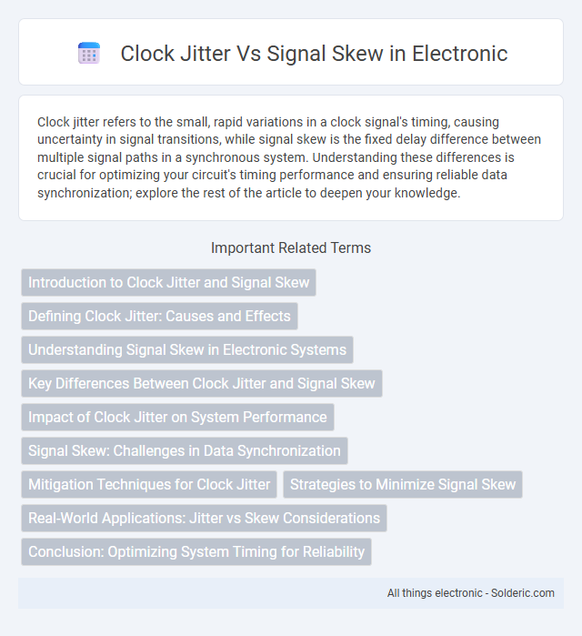
Clock jitter refers to the small, rapid variations in a clock signal's timing, causing uncertainty in signal transitions, while signal skew is the fixed delay difference between multiple signal paths in a synchronous system. Understanding these differences is crucial for optimizing your circuit's timing performance and ensuring reliable data synchronization; explore the rest of the article to deepen your knowledge.
Comparison Table
| Aspect | Clock Jitter | Signal Skew |
|---|---|---|
| Definition | Random or deterministic timing variations in clock signal edges. | Time difference in arrival of the same signal at multiple destinations. |
| Cause | Noise, power supply fluctuations, temperature variations, phase noise. | Trace length differences, varying path delays, mismatched routing. |
| Impact | Degrades timing accuracy; may cause setup and hold time violations. | Leads to data misalignment and timing errors in synchronous circuits. |
| Measurement | RMS jitter (Root Mean Square), peak-to-peak jitter. | Time difference measured in picoseconds or nanoseconds between signals. |
| Control Techniques | Use of low jitter oscillators, phase-locked loops (PLLs), filtering. | Careful PCB layout, matched trace lengths, delay compensation. |
| Category | Dynamic timing variation | Deterministic timing offset |
Introduction to Clock Jitter and Signal Skew
Clock jitter represents the random variations in the timing of clock signal edges, affecting the precision of digital circuit operations. Signal skew refers to the systematic difference in arrival times of signals at different components due to path length variations or circuit delays. Both clock jitter and signal skew critically impact timing accuracy and synchronization in high-speed electronic systems, influencing overall system performance and reliability.
Defining Clock Jitter: Causes and Effects
Clock jitter refers to the small, rapid variations in the timing of a clock signal's edges, caused by factors such as power supply noise, electromagnetic interference, and intrinsic device noise. These timing fluctuations can lead to data errors, reduce signal integrity, and impact the overall performance of high-speed digital systems. Understanding clock jitter is crucial for optimizing your system's timing accuracy and minimizing signal degradation compared to signal skew, which deals with timing differences between multiple clock signals.
Understanding Signal Skew in Electronic Systems
Signal skew in electronic systems refers to the timing difference between signals intended to be simultaneous, causing synchronization challenges that affect overall circuit performance. Unlike clock jitter, which is random variation in signal timing, signal skew is usually a systematic delay caused by unequal path lengths, fabrication mismatches, or temperature variations across components. Accurate management of signal skew is crucial for high-speed digital circuits to ensure data integrity and minimize setup and hold time violations.
Key Differences Between Clock Jitter and Signal Skew
Clock jitter refers to the short-term variations in the timing of a clock signal's edges, causing uncertainty in signal transitions and impacting data integrity at high speeds. Signal skew describes the time difference or delay between signals intended to switch simultaneously within the same clock cycle, often due to differences in path lengths or routing in PCB design. Understanding these key differences helps you optimize timing analysis and improve system reliability in digital circuits.
Impact of Clock Jitter on System Performance
Clock jitter introduces timing uncertainty by causing variations in clock signal edges, directly affecting system synchronization and data integrity. Unlike signal skew, which is a fixed delay difference between clock paths, jitter leads to unpredictable timing errors that degrade clock-data alignment, increasing the bit error rate and reducing overall system reliability. High jitter levels stress timing margins in high-speed digital circuits, impacting setup and hold times critical for robust performance in microprocessors and communication systems.
Signal Skew: Challenges in Data Synchronization
Signal skew poses significant challenges in data synchronization by causing timing mismatches between clock signals across different parts of a digital system, leading to data integrity errors and reduced system performance. Variations in signal path lengths and propagation delays create uneven arrival times of clock edges, making precise timing alignment critical in high-speed communication and circuit design. Addressing signal skew requires careful PCB layout, clock distribution network optimization, and the use of delay-locked loops (DLLs) or phase-locked loops (PLLs) to ensure synchronized data capture and reliable operation.
Mitigation Techniques for Clock Jitter
Mitigation techniques for clock jitter primarily involve using phase-locked loops (PLLs) and delay-locked loops (DLLs) to stabilize and synchronize timing signals in digital circuits. Implementing low-jitter clock sources and employing signal conditioning methods, such as filtering and shielding, effectively reduce noise-induced variations. Understanding these approaches enables you to enhance timing accuracy and improve overall system performance by minimizing the impact of clock jitter.
Strategies to Minimize Signal Skew
Minimizing signal skew involves precise routing of high-speed signals using matched trace lengths on PCB layouts to ensure synchronized arrival times. Implementing controlled impedance and proper termination reduces reflections and timing variations that contribute to skew. Advanced techniques like differential signaling and the use of programmable delay elements further enhance timing alignment in complex clock distribution networks.
Real-World Applications: Jitter vs Skew Considerations
In high-speed digital circuits, clock jitter affects timing accuracy by causing unpredictable variations in the clock signal period, leading to data setup and hold time violations. Signal skew, the fixed delay difference between clock signals arriving at different components, impacts synchronization across large-scale systems such as multi-core processors and FPGAs. Real-world applications prioritize minimizing jitter for low-latency environments like high-frequency trading, while skew management is critical in synchronous communication systems to ensure consistent timing alignment.
Conclusion: Optimizing System Timing for Reliability
Clock jitter and signal skew critically impact system timing accuracy and reliability in high-speed digital circuits. Minimizing clock jitter ensures stable clock edges, reducing timing uncertainty, while controlling signal skew aligns data arrival times, preventing setup and hold time violations. Optimizing both parameters through precise clock distribution and synchronized routing enhances overall system performance and reliability.
clock jitter vs signal skew Infographic