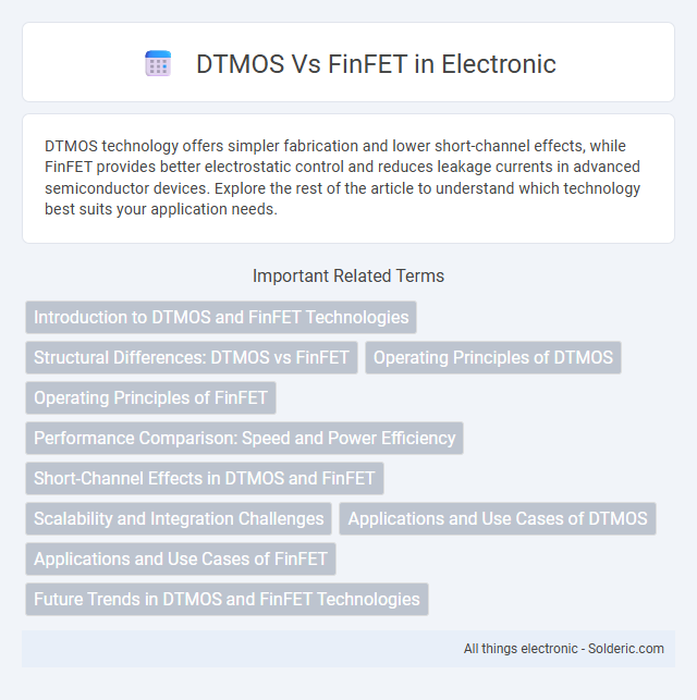
DTMOS technology offers simpler fabrication and lower short-channel effects, while FinFET provides better electrostatic control and reduces leakage currents in advanced semiconductor devices. Explore the rest of the article to understand which technology best suits your application needs.
Comparison Table
| Feature | DTMOS (Dynamic Threshold MOS) | FinFET (Fin Field Effect Transistor) |
|---|---|---|
| Technology Type | Planar transistor with dynamic threshold adjustment | 3D multi-gate transistor structure |
| Threshold Voltage | Variable, changes dynamically to reduce leakage | Fixed, inherently low threshold for improved control |
| Leakage Current | Reduced via adaptive threshold | Significantly low due to gate control |
| Drive Current | Moderate, improved over traditional MOS | High, enhanced channel control |
| Short Channel Effects | Partially mitigated by dynamic threshold | Strongly suppressed by 3D structure |
| Fabrication Complexity | Relatively simple, planar process | High complexity due to 3D patterning |
| Scaling Capability | Limited for advanced nodes | Excellent for sub-14 nm technologies |
| Power Efficiency | Improved via threshold modulation | Superior, due to reduced leakage and better control |
| Application | Low-power circuits, adaptive threshold control | High-performance processors, advanced logic |
Introduction to DTMOS and FinFET Technologies
DTMOS (Dynamic Threshold MOS) technology enhances transistor switching speed by dynamically adjusting the threshold voltage, improving power efficiency in integrated circuits. FinFET (Fin Field-Effect Transistor) technology uses a 3D vertical fin structure to increase channel control and reduce leakage current, enabling superior performance for nanoscale semiconductor devices. Your choice between DTMOS and FinFET depends on specific application needs, balancing speed, power consumption, and fabrication complexity.
Structural Differences: DTMOS vs FinFET
DTMOS (Dynamic Threshold MOS) transistors utilize a body biasing technique where the substrate or well potential dynamically adjusts to control the threshold voltage, enabling improved leakage control and performance. In contrast, FinFET (Fin Field-Effect Transistor) devices feature a three-dimensional, fin-shaped channel wrapped by the gate on multiple sides, providing enhanced electrostatic control and reduced short-channel effects. The key structural difference lies in DTMOS relying on substrate bias manipulation within planar CMOS architecture, whereas FinFET employs a vertical fin structure for superior gate control and scalability.
Operating Principles of DTMOS
DTMOS (Dynamic Threshold MOS) operates by dynamically adjusting the threshold voltage through substrate biasing, which enhances drive current and reduces leakage power. This technique enables improved switching performance compared to conventional FinFETs, which rely on a multi-gate structure to control channel conduction and suppress short-channel effects. By modulating the body potential in real-time, DTMOS maintains high speed and low power consumption, optimizing transistor operation for low-voltage applications.
Operating Principles of FinFET
FinFETs operate by wrapping a thin silicon fin with a gate electrode, enabling enhanced electrostatic control over the channel compared to planar transistors. This 3D structure reduces short-channel effects by controlling the current through multiple sides of the fin, improving performance and power efficiency. The gate's ability to modulate the channel from more than one direction enables higher drive current and lower leakage, making FinFETs suitable for advanced semiconductor nodes.
Performance Comparison: Speed and Power Efficiency
DTMOS devices exhibit lower threshold voltages leading to higher switching speeds compared to FinFETs, enhancing overall performance in high-speed applications. FinFET technology offers superior power efficiency due to its better control of short-channel effects and reduced leakage currents, making it favorable for low-power designs. Performance trade-offs between DTMOS and FinFET depend on the specific use case, with DTMOS excelling in speed and FinFET optimizing power consumption.
Short-Channel Effects in DTMOS and FinFET
DTMOS devices exhibit more pronounced short-channel effects (SCEs) such as threshold voltage roll-off and drain-induced barrier lowering due to their planar structure and direct substrate coupling. In contrast, FinFETs offer superior control over the channel potential through their three-dimensional multi-gate architecture, significantly suppressing short-channel effects and enabling better scalability. The enhanced electrostatic integrity of FinFETs minimizes leakage currents and improves device performance in nanoscale technology nodes compared to DTMOS.
Scalability and Integration Challenges
DTMOS technology faces scalability limitations as device dimensions shrink below 5nm, impacting short-channel control and increasing leakage currents, whereas FinFETs provide superior electrostatic control with 3D fin structures that enhance scalability down to 3nm nodes. Integration challenges for DTMOS include complex body biasing and variability issues in large-scale circuits, while FinFETs demand sophisticated manufacturing steps like multi-patterning and fin etching, raising fabrication complexity and cost. Your choice between DTMOS and FinFET should consider these scalability trade-offs and integration hurdles to optimize performance and yield in advanced semiconductor nodes.
Applications and Use Cases of DTMOS
DTMOS technology excels in ultra-low-power applications such as wearable devices, IoT sensors, and biomedical implants, where energy efficiency is critical for extended battery life. Unlike FinFETs, which dominate high-performance computing and mobile processors due to their superior drive current and scalability, DTMOS transistors leverage dynamic threshold voltage modulation to reduce leakage currents and enhance switching speed in low-voltage environments. Your choice of semiconductor technology will depend on the specific power consumption and performance requirements of the application, with DTMOS offering advantages in scenarios demanding minimal power dissipation and cost-effectiveness.
Applications and Use Cases of FinFET
FinFET technology is extensively used in high-performance microprocessors, mobile devices, and advanced artificial intelligence chips due to its superior control over short-channel effects and reduced leakage currents. Its widespread adoption in semiconductor manufacturing enables enhanced power efficiency and scalability for applications requiring high transistor density, such as data centers and 5G communication systems. FinFET's robustness in dynamic environments makes it the preferred choice for both consumer electronics and automotive safety systems.
Future Trends in DTMOS and FinFET Technologies
DTMOS technology continues to evolve with advancements in dynamic threshold control, enhancing power efficiency for ultra-low voltage applications. FinFET technology is trending towards nanosheet and gate-all-around (GAA) transistors, promising improved electrostatic control and scalability beyond the 3nm node. Your choice between DTMOS and FinFET will depend on specific performance requirements and the future integration of these emerging transistor architectures in semiconductor devices.
DTMOS vs FinFET Infographic