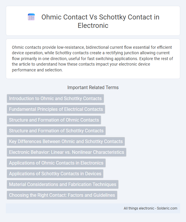
Ohmic contacts provide low-resistance, bidirectional current flow essential for efficient device operation, while Schottky contacts create a rectifying junction allowing current flow primarily in one direction, useful for fast switching applications. Explore the rest of the article to understand how these contacts impact your electronic device performance and selection.
Comparison Table
| Feature | Ohmic Contact | Schottky Contact |
|---|---|---|
| Definition | Low-resistance contact allowing current flow in both directions | Metal-semiconductor junction with rectifying behavior |
| Current Flow | Bidirectional, linear I-V characteristics | Unidirectional, nonlinear I-V characteristics (rectifying) |
| Barrier Type | Negligible or no barrier | Schottky barrier at the metal-semiconductor interface |
| Application | Electrical contacts in semiconductor devices to minimize resistance | Diodes, Schottky rectifiers, detectors, high-speed switches |
| Material Interaction | Highly doped semiconductor region to form ohmic behavior | Metal forms a barrier due to work function difference |
| Example Materials | AuGe/Ni on n-type GaAs | Pt on n-type Silicon |
| Resistance | Low contact resistance | Higher contact resistance with voltage-dependent behavior |
| Temperature Sensitivity | Relatively stable | More sensitive to temperature variations |
Introduction to Ohmic and Schottky Contacts
Ohmic and Schottky contacts are essential components in semiconductor devices, influencing current flow and device performance. Ohmic contacts provide a low-resistance, linear current-voltage relationship, enabling efficient charge carrier injection without energy barriers. Schottky contacts, formed between a metal and a semiconductor, create a rectifying junction that allows current to flow primarily in one direction, critical for devices like Schottky diodes and metal-semiconductor field-effect transistors (MESFETs).
Fundamental Principles of Electrical Contacts
Ohmic contacts are designed to provide a low-resistance, linear current-voltage relationship by allowing charge carriers to flow freely between the metal and semiconductor without significant energy barriers. Schottky contacts, in contrast, form a rectifying junction with a metal-semiconductor interface that creates a Schottky barrier, resulting in nonlinear current flow and selective carrier movement. Understanding these fundamental principles is crucial for optimizing Your device's electrical performance in applications such as diodes and transistors.
Structure and Formation of Ohmic Contacts
Ohmic contacts are formed by creating a low-resistance interface between a metal and a semiconductor, often achieved through alloying or doping to reduce the Schottky barrier height and enable efficient carrier injection. Unlike Schottky contacts, which exhibit rectifying behavior due to a built-in potential barrier, Ohmic contacts ensure linear current-voltage characteristics essential for device operation. Your semiconductor device's performance depends heavily on the precise structure and quality of these contacts to minimize energy loss and enhance electrical conductivity.
Structure and Formation of Schottky Contacts
Schottky contacts consist of a metal-semiconductor junction formed by depositing a metal with a specific work function onto an n-type or p-type semiconductor, creating a rectifying barrier that controls charge carrier flow. The barrier height depends on the metal's work function and the semiconductor's electron affinity, influencing the contact's electrical characteristics by enabling current flow primarily in one direction. Unlike ohmic contacts, Schottky contacts form without heavily doped semiconductor regions, relying on the intrinsic properties of the metal-semiconductor interface to establish their rectifying behavior.
Key Differences Between Ohmic and Schottky Contacts
Ohmic contacts provide a low-resistance, linear I-V characteristic essential for efficient current flow in semiconductor devices, while Schottky contacts exhibit rectifying behavior due to a metal-semiconductor junction forming a barrier. The key difference lies in their electrical behavior: Ohmic contacts allow bidirectional current with minimal voltage drop, whereas Schottky contacts allow current primarily in one direction, creating a diode-like response. Material choice and barrier height at the interface critically impact these contact types, influencing device performance in applications like transistors and sensors.
Electronic Behavior: Linear vs. Nonlinear Characteristics
Ohmic contacts exhibit linear current-voltage characteristics, allowing efficient charge carrier flow with minimal resistance, enabling reliable electrical connections in semiconductor devices. Schottky contacts demonstrate nonlinear behavior due to the metal-semiconductor barrier, resulting in rectifying properties that control current flow direction and magnitude. Understanding these electronic behaviors helps optimize Your device performance depending on whether linear conduction or controlled rectification is required.
Applications of Ohmic Contacts in Electronics
Ohmic contacts are essential in electronic devices for providing low-resistance, non-rectifying connections between metal and semiconductor materials, enabling efficient current flow in components such as transistors, diodes, and integrated circuits. These contacts are critical in power electronics, enabling high current densities without significant voltage drops or heating, which ensures device reliability and performance. Ohmic contacts are also widely used in sensors and photovoltaic cells to facilitate stable electrical interfacing and improve signal accuracy.
Applications of Schottky Contacts in Devices
Schottky contacts are widely used in high-speed and high-frequency devices due to their low forward voltage drop and fast switching capabilities, making them ideal for Schottky diodes and radio-frequency mixers. Their unique metal-semiconductor junction enables efficient charge carrier transport, which enhances the performance of power rectifiers and solar cells. Your choice of Schottky contacts significantly impacts device efficiency in applications requiring rapid response and minimal energy loss.
Material Considerations and Fabrication Techniques
Ohmic contacts require materials with work functions closely matching the semiconductor to minimize contact resistance, commonly using metals like Au, Ti, or Ni combined with heavy doping techniques to achieve linear current-voltage characteristics. Schottky contacts utilize metals such as Pt, Pd, or Au that form a rectifying barrier with the semiconductor, relying on precise deposition methods like sputtering or evaporation to control barrier height and interface quality. Fabrication techniques for both contacts involve careful surface cleaning, thermal annealing, and sometimes interfacial layer engineering to optimize electrical performance and device reliability.
Choosing the Right Contact: Factors and Guidelines
Choosing the right contact between ohmic and Schottky types depends primarily on your device's required electrical characteristics and performance goals. Ohmic contacts provide low-resistance, linear current flow ideal for steady-state conduction, while Schottky contacts offer rectifying behavior with fast switching and low forward voltage drop, beneficial in high-frequency and power-sensitive applications. Evaluating factors such as contact resistance, barrier height, and semiconductor material compatibility ensures optimal device efficiency and reliability.
Ohmic contact vs Schottky contact Infographic