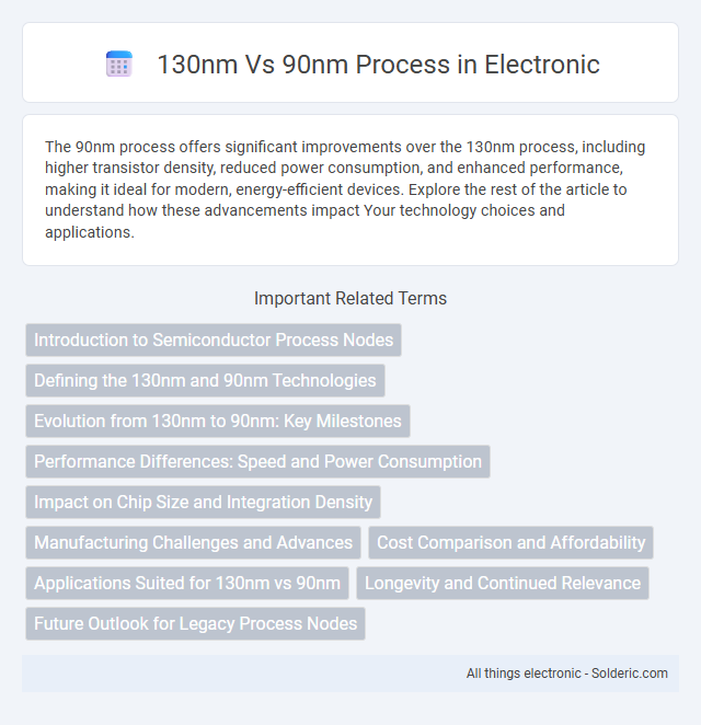
The 90nm process offers significant improvements over the 130nm process, including higher transistor density, reduced power consumption, and enhanced performance, making it ideal for modern, energy-efficient devices. Explore the rest of the article to understand how these advancements impact Your technology choices and applications.
Comparison Table
| Feature | 130nm Process | 90nm Process |
|---|---|---|
| Technology Node | 130 nanometers | 90 nanometers |
| Transistor Density | Lower density | Higher density |
| Gate Length | ~130nm | ~90nm |
| Power Consumption | Higher power usage | Lower power usage |
| Switching Speed | Slower transistor switching | Faster transistor switching |
| Leakage Current | Moderate leakage | Higher leakage, mitigated by design |
| Cost of Fabrication | Lower manufacturing cost | Higher manufacturing cost |
| Application | Legacy and low cost devices | Performance-critical and energy-efficient chips |
Introduction to Semiconductor Process Nodes
The 130nm and 90nm semiconductor process nodes represent critical advancements in chip fabrication, with 90nm offering smaller transistor features that enhance performance and power efficiency. You benefit from tighter geometries at 90nm, enabling higher transistor density and faster switching speeds compared to the 130nm process. These nodes mark significant steps in Moore's Law, driving innovation in microprocessors, memory chips, and integrated circuits for diverse electronic applications.
Defining the 130nm and 90nm Technologies
The 130nm and 90nm processes refer to semiconductor manufacturing technologies that define the minimum feature size of transistors on a chip, with 90nm representing a more advanced, smaller node compared to 130nm. The 130nm technology typically offers lower fabrication costs and proven reliability, while 90nm enables higher transistor density, improved performance, and reduced power consumption for more efficient integrated circuits. Your choice between 130nm and 90nm should align with your desired balance between cost, performance, and power efficiency in electronic device design.
Evolution from 130nm to 90nm: Key Milestones
The evolution from 130nm to 90nm process technology marked significant advancements in semiconductor manufacturing, including reduced transistor size, enhanced performance, and lower power consumption. Key milestones involved the introduction of advanced lithography techniques, improved materials like high-k dielectrics, and refined doping processes that boosted device reliability and integration density. Your products benefit from these developments through faster speeds, greater efficiency, and compact design possibilities.
Performance Differences: Speed and Power Consumption
The 90nm process technology offers higher transistor density and lower gate capacitance compared to the 130nm node, resulting in increased switching speeds and improved overall performance. Power consumption is significantly reduced in the 90nm process due to lower operating voltages and leakage currents, enhancing energy efficiency for integrated circuits. These advantages make 90nm more suitable for high-speed, low-power applications in modern semiconductor devices.
Impact on Chip Size and Integration Density
The transition from 130nm to 90nm process technology significantly reduces chip size by enabling finer transistor geometries and tighter packing of components. This improved integration density allows more functionality to be placed on a single chip, enhancing performance and reducing power consumption. Your designs can benefit from cost savings and increased processing capabilities due to the higher transistor count achievable with the 90nm process.
Manufacturing Challenges and Advances
The 130nm process node faced significant manufacturing challenges, including photolithography resolution limits and increased defect rates, which hindered yield and scaling efficiency. Advances in immersion lithography, improved etching techniques, and enhanced process controls enabled the transition to the 90nm node, allowing finer transistor geometries and higher integration density. Innovations such as strained silicon and high-k dielectric materials at 90nm also addressed short-channel effects and leakage currents, enhancing device performance and power efficiency.
Cost Comparison and Affordability
The 130nm process technology offers lower manufacturing costs compared to 90nm, primarily due to less expensive equipment and higher yield rates, making it more affordable for low-to-mid volume production. Although 90nm provides better performance and power efficiency, its increased fabrication complexity and higher mask costs result in significantly higher overall expenses. For cost-sensitive projects and applications where cutting-edge performance is not critical, 130nm remains the more economically viable option.
Applications Suited for 130nm vs 90nm
130nm process technology is well-suited for cost-sensitive applications such as automotive electronics, power management ICs, and embedded systems where moderate performance and lower manufacturing costs are prioritized. The 90nm process excels in high-performance computing, mobile processors, and advanced consumer electronics due to improved transistor speed, reduced power consumption, and higher integration density. Both technologies serve distinct market segments, with 130nm favored for robust reliability and 90nm chosen for speed-critical and power-efficient designs.
Longevity and Continued Relevance
The 130nm and 90nm process technologies both maintain longevity and continued relevance due to their balance of cost efficiency, proven reliability, and compatibility with a wide range of applications, including automotive and industrial sectors. While 90nm offers improved performance and power efficiency over 130nm, the 130nm node still thrives in scenarios requiring robust manufacturing yields and established design infrastructures. Continued demand for legacy semiconductor devices ensures that both process nodes remain critical in sustaining diverse electronics ecosystems.
Future Outlook for Legacy Process Nodes
Legacy process nodes such as 130nm and 90nm remain crucial for applications requiring high reliability and lower production costs, including automotive, industrial, and IoT devices. The future outlook emphasizes continued demand driven by these sectors, with enhancements in design methodologies and embedded technologies to maximize performance within existing constraints. Your choice between 130nm and 90nm processes will depend on balancing cost-efficiency with specific performance and integration needs.
130nm vs 90nm Process Infographic