Microbump and flip-chip technologies offer distinct advantages for semiconductor packaging, with microbumps providing finer pitch and higher density interconnections, while flip-chip delivers robust mechanical stability and efficient heat dissipation. Explore the rest of this article to understand which method best suits your advanced electronic design needs.
Comparison Table
| Feature | Microbump | Flip-chip |
|---|---|---|
| Definition | Miniature solder bumps used for die-to-wafer or die-to-die interconnects | Method of mounting semiconductor die by flipping and connecting via solder bumps |
| Bump Size | Typically 10-20 um diameter | Larger, around 50-100 um diameter |
| Pitch | Finer pitch, usually under 40 um | Coarser pitch, generally over 100 um |
| Applications | High-density 3D IC stacking and wafer-level packaging | Standard IC packaging and chip-to-substrate mounting |
| Electrical Performance | Lower inductance and resistance due to shorter interconnects | Higher inductance and resistance, suitable for less dense designs |
| Manufacturing Complexity | Higher due to precise bump formation and alignment | Lower complexity, mature process with established infrastructure |
| Cost | Higher cost per unit area | Generally lower cost with mass production |
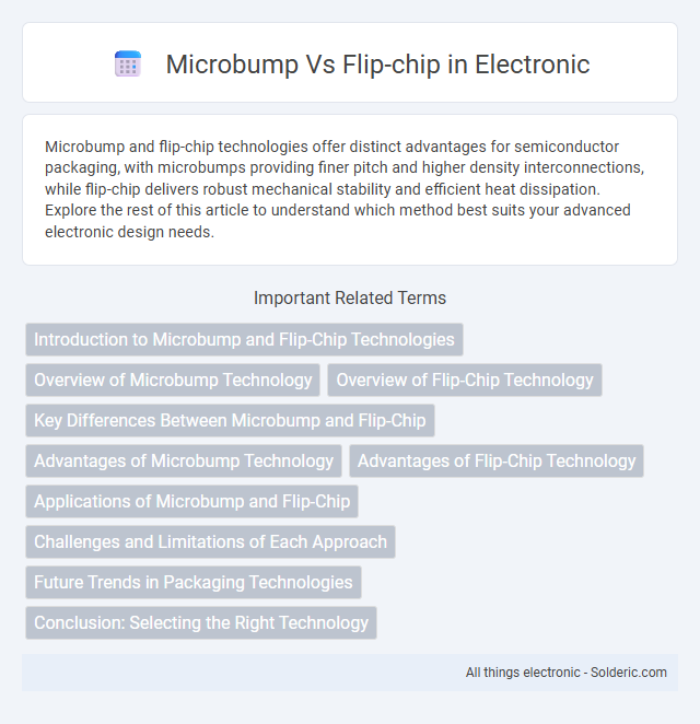
Introduction to Microbump and Flip-Chip Technologies
Microbump and Flip-Chip are advanced semiconductor packaging technologies used to enhance electrical performance and miniaturization. Microbump technology utilizes tiny solder bumps, typically measuring less than 20 micrometers, to create high-density interconnects ideal for stacking dies in 3D ICs. Flip-Chip involves flipping the silicon chip to directly connect to the substrate with larger solder bumps, offering improved signal integrity and thermal management compared to traditional wire bonding.
Overview of Microbump Technology
Microbump technology employs micro-sized solder bumps to create high-density interconnects between semiconductor dies, enabling improved electrical performance and reduced package size compared to traditional flip-chip methods. These microbumps, typically below 20 microns in diameter, facilitate finer pitch connections, enhancing signal integrity and thermal management in advanced 3D IC packaging. This approach supports next-generation applications such as high-bandwidth memory (HBM) and heterogeneous integration by providing scalable and reliable chip-to-chip bonding solutions.
Overview of Flip-Chip Technology
Flip-chip technology uses solder bumps directly on the chip pads to create a high-density electrical connection between the semiconductor die and the substrate, enabling improved electrical performance and heat dissipation compared to traditional wire bonding. Microbump technology, a variant of flip-chip, employs smaller bumps typically used in 3D integrated circuits and advanced packaging to achieve higher interconnect density and enhanced signal integrity. This method allows for more compact designs and superior bandwidth in applications such as high-speed communication and advanced microprocessors.
Key Differences Between Microbump and Flip-Chip
Microbump technology features smaller, finer pitch interconnects typically used for high-density 3D IC stacking, while flip-chip employs larger solder bumps for direct die-to-substrate connections. Microbump offers enhanced electrical performance and thermal management due to reduced parasitics and shorter interconnects, contrasting with flip-chip's broader usage in traditional package assemblies. Packaging cost and wafer-level processing complexity also differentiate microbump, which demands advanced fabrication, from flip-chip's relatively mature and scalable manufacturing process.
Advantages of Microbump Technology
Microbump technology offers significant advantages over traditional flip-chip methods, including higher interconnect density and improved electrical performance due to smaller and more precise solder bumps. This technology enables finer pitch connections, which enhance signal integrity and reduce parasitic capacitance, making it ideal for advanced semiconductor packaging. You benefit from better thermal management and increased reliability in high-performance applications with microbump's superior mechanical stability and reduced stress on the substrate.
Advantages of Flip-Chip Technology
Flip-chip technology offers superior electrical performance by enabling shorter interconnects and reduced parasitic inductance compared to microbump methods. This approach supports higher input/output (I/O) density and improved thermal management, which enhances the reliability and speed of your semiconductor devices. Furthermore, flip-chip allows for more compact designs and better mechanical stability, making it ideal for advanced packaging applications in high-performance electronics.
Applications of Microbump and Flip-Chip
Microbump technology is widely applied in 3D integrated circuits (3D ICs) for high-density stacking of memory chips and logic dies, enhancing performance in smartphones, servers, and high-performance computing devices. Flip-chip is extensively used in consumer electronics, automotive sensors, and RF modules, providing superior electrical performance and thermal management by directly connecting the die to the substrate. Understanding the applications of Microbump and Flip-Chip helps optimize Your device designs for improved speed, power efficiency, and miniaturization.
Challenges and Limitations of Each Approach
Microbump technology faces challenges such as limited current-carrying capacity and thermal dissipation issues due to smaller bump sizes, which can affect reliability in high-power applications. Flip-chip assembly encounters limitations in handling finer pitch interconnects and managing warpage during reflow processes, potentially leading to misalignment and solder joint defects. Both approaches require careful consideration of substrate material compatibility and mechanical stress to ensure long-term performance and yield.
Future Trends in Packaging Technologies
Microbump technology is advancing towards enabling finer pitch interconnections crucial for high-density 3D integration, offering superior electrical performance and thermal management compared to traditional flip-chip methods. Flip-chip packaging continues to evolve with enhanced underfill materials and advanced substrate designs, supporting higher input/output counts and improved reliability for next-generation semiconductor devices. Emerging trends highlight the convergence of microbump and flip-chip techniques with heterogeneous integration, driving innovations in system-in-package (SiP) solutions and enabling compact, high-performance electronic assemblies.
Conclusion: Selecting the Right Technology
Microbump technology offers finer pitch capabilities and is ideal for high-density, advanced semiconductor packaging, while flip-chip provides robust mechanical stability and cost-effective solutions for broader applications. Choosing between microbump and flip-chip depends on factors like performance requirements, package size constraints, and manufacturing cost considerations. Evaluating thermal management, signal integrity, and scalability ensures the selected interconnect technology aligns with the specific needs of the electronic device.
Microbump vs Flip-chip Infographic