Direct band gap semiconductors allow electrons to directly recombine with holes, emitting light efficiently, making them ideal for optoelectronic devices like LEDs and lasers. Understanding the differences between direct and indirect band gap semiconductors will help you grasp their applications and performance, so read on to explore these essential concepts further.
Comparison Table
| Feature | Direct Band Gap Semiconductor | Indirect Band Gap Semiconductor |
|---|---|---|
| Electron Transition | Conduction band minimum and valence band maximum at the same momentum | Conduction band minimum and valence band maximum at different momentum |
| Photon Emission Efficiency | High, efficient light emission (e.g., LEDs, laser diodes) | Low, inefficient light emission |
| Common Materials | Gallium arsenide (GaAs), Indium phosphide (InP) | Silicon (Si), Germanium (Ge) |
| Applications | Optoelectronics, photovoltaics, LED technology | Microelectronics, power devices, photovoltaics (less efficient) |
| Recombination Type | Direct recombination without phonon involvement | Phonon-assisted recombination due to momentum mismatch |
| Energy Band Structure | Direct band gap energy (Eg) is minimum | Indirect band gap energy (Eg) involves phonon participation |
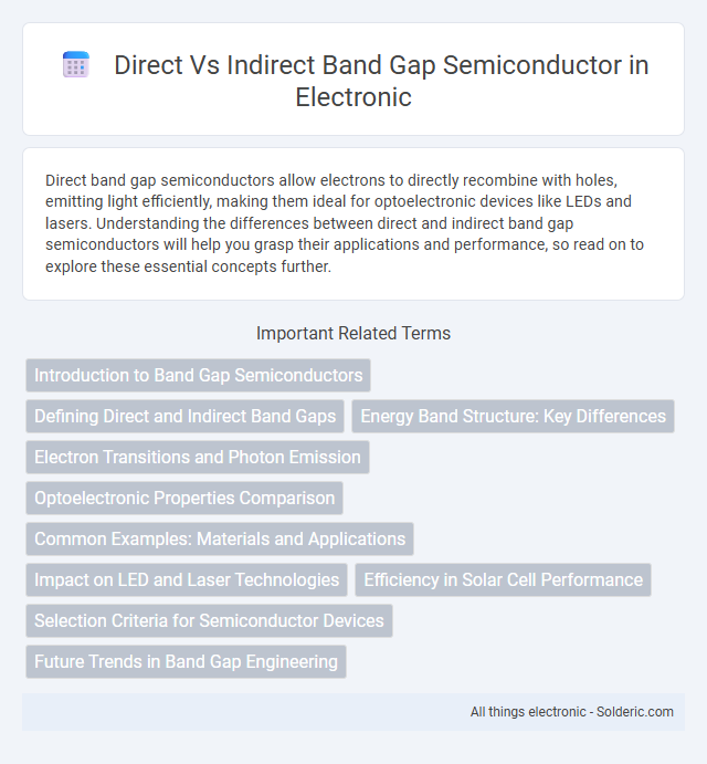
Introduction to Band Gap Semiconductors
Band gap semiconductors are materials characterized by an energy gap between the valence band and conduction band, determining their electrical conductivity. Direct band gap semiconductors allow electrons to transition directly between bands by emitting or absorbing photons, making them ideal for optoelectronic devices such as LEDs and laser diodes. Indirect band gap semiconductors require a change in momentum involving phonons during electron transitions, resulting in less efficient light emission but often providing better thermal and electrical properties for applications like solar cells and transistors.
Defining Direct and Indirect Band Gaps
Direct band gap semiconductors have their conduction band minimum and valence band maximum aligned at the same momentum value, allowing electrons to directly recombine with holes and emit photons efficiently. Indirect band gap semiconductors feature a momentum mismatch between these band edges, requiring phonon involvement for electron-hole recombination, which reduces optical emission efficiency. Understanding this distinction is crucial for optimizing your design in optoelectronic applications like LEDs and lasers.
Energy Band Structure: Key Differences
Direct band gap semiconductors have their conduction band minimum and valence band maximum aligned at the same momentum (k-vector), enabling electrons to recombine with holes directly and emit photons efficiently. Indirect band gap semiconductors exhibit a momentum mismatch between the conduction band minimum and valence band maximum, requiring phonon involvement for electron-hole recombination, which reduces optical emission efficiency. This fundamental difference in energy band structure critically affects their applications in optoelectronic devices such as LEDs and laser diodes versus electronic devices like transistors.
Electron Transitions and Photon Emission
In direct band gap semiconductors, electrons transition from the conduction band to the valence band while conserving momentum, allowing efficient photon emission critical for optoelectronic devices like LEDs and laser diodes. Indirect band gap semiconductors require a phonon to assist in the electron transition due to momentum mismatch, resulting in less efficient photon emission and reduced light-emitting capabilities. Understanding these electron transitions can help you select the right semiconductor material for applications involving photon emission and light absorption.
Optoelectronic Properties Comparison
Direct band gap semiconductors efficiently emit light due to their electron transitions occurring at the same momentum, making them ideal for LEDs, laser diodes, and photodetectors. Indirect band gap semiconductors exhibit lower radiative recombination rates because electron transitions require phonon assistance to conserve momentum, reducing their light emission efficiency but offering advantages in electronic applications like solar cells. The superior optoelectronic properties of direct band gap materials are critical for high-performance optoelectronic devices, while indirect band gap materials provide better thermal stability and cost-effectiveness.
Common Examples: Materials and Applications
Gallium arsenide (GaAs) and indium phosphide (InP) are common direct band gap semiconductors widely used in optoelectronic devices like LEDs, laser diodes, and high-speed photodetectors due to their efficient light emission properties. Silicon and germanium, representing indirect band gap semiconductors, dominate microelectronics and integrated circuits where light emission is not critical because their electron transitions require phonon assistance, making them less efficient for optoelectronic applications. Emerging materials like transition metal dichalcogenides (TMDCs) exhibit direct band gaps in monolayer forms, enabling applications in flexible and nanoscale photonic devices.
Impact on LED and Laser Technologies
Direct band gap semiconductors, such as gallium arsenide (GaAs), enable efficient electron-hole recombination, resulting in high light emission efficiency critical for LED and laser technologies. Indirect band gap materials, like silicon, exhibit lower photon emission efficiency due to momentum mismatch requiring phonon assistance, limiting their use in optoelectronic devices. Innovations in direct band gap materials have driven advancements in high-performance LEDs and semiconductor lasers with enhanced brightness and wavelength precision.
Efficiency in Solar Cell Performance
Direct band gap semiconductors exhibit higher efficiency in solar cell performance due to their ability to directly absorb and emit photons, enabling better light absorption and electron-hole pair generation. Indirect band gap materials require phonon interaction for electron transitions, resulting in lower absorption efficiency and necessitating thicker layers to capture sunlight effectively. Your solar cell design benefits significantly from utilizing direct band gap materials to maximize energy conversion efficiency and reduce material thickness.
Selection Criteria for Semiconductor Devices
Direct band gap semiconductors are preferred for optoelectronic devices such as LEDs and laser diodes due to their efficient electron-hole recombination, producing strong light emission. Indirect band gap semiconductors, while less efficient in light emission, offer better thermal conductivity and are commonly used in electronic devices requiring high-speed performance and heat dissipation. Your choice of semiconductor material should consider the specific application requirements, balancing optical efficiency and electrical conductivity to optimize device performance.
Future Trends in Band Gap Engineering
Future trends in band gap engineering emphasize the development of quantum dot and perovskite materials to enhance optoelectronic device efficiency by exploiting tunable direct band gaps. Advances in two-dimensional semiconductors, such as transition metal dichalcogenides (TMDCs), enable precise control over direct and indirect band gap transitions through strain engineering and layer number variation. Integration of machine learning algorithms accelerates the discovery of novel compounds with tailored band gap properties for applications in photovoltaics, LEDs, and laser technologies.
Direct vs Indirect Band Gap Semiconductor Infographic