Thermal oxidation involves heating a silicon wafer in an oxygen-rich environment to create a uniform and dense oxide layer, ideal for high-quality insulating films in semiconductor devices. Plasma oxidation uses reactive plasma to oxidize surfaces at lower temperatures, offering faster processing and better control over thin oxide layers, making it suitable for delicate or temperature-sensitive substrates; explore the rest of this article to understand which method best fits Your needs.
Comparison Table
| Feature | Thermal Oxidation | Plasma Oxidation |
|---|---|---|
| Process | Oxidation using high-temperature steam or dry oxygen | Oxidation by reactive oxygen plasma at low temperature |
| Temperature Range | 800degC to 1200degC | 100degC to 400degC |
| Oxide Quality | High-quality, dense SiO2 layer | Typically thinner and less dense oxide layer |
| Oxidation Rate | Slower, controlled growth | Faster at low temperatures |
| Equipment | Furnaces with steam or dry oxygen flow | Plasma reactors generating oxygen plasma |
| Applications | Gate oxides, high-quality insulating layers in semiconductor fabrication | Surface cleaning, shallow oxide growth, modification of materials sensitive to high heat |
| Advantages | Excellent oxide uniformity and reliability | Low thermal budget, selective oxidation possible |
| Disadvantages | High thermal budget, longer process time | Generally lower oxide quality, possible damage due to plasma |
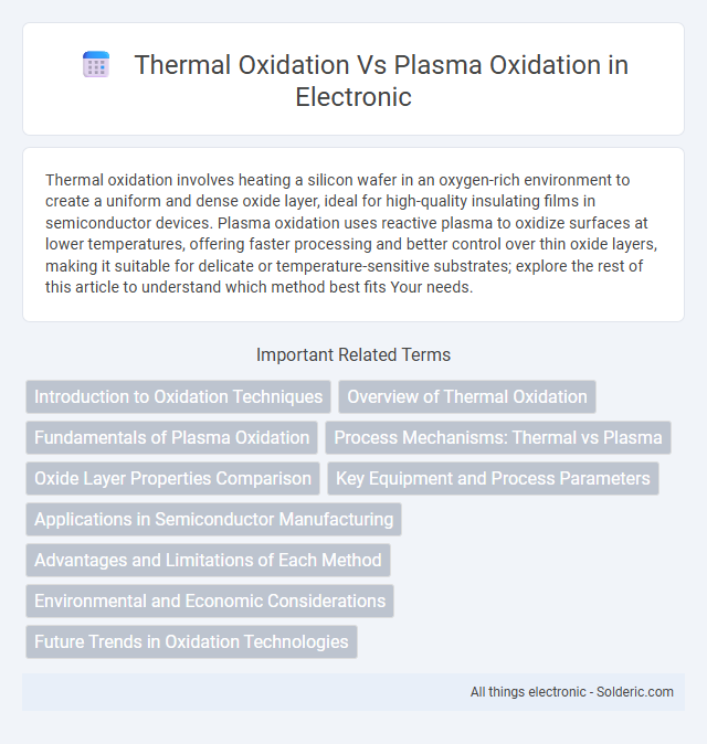
Introduction to Oxidation Techniques
Thermal oxidation involves heating silicon wafers in an oxygen-rich environment at temperatures between 900degC and 1200degC to grow a uniform silicon dioxide layer, critical for semiconductor device fabrication. Plasma oxidation, on the other hand, utilizes reactive oxygen plasma generated at lower temperatures around 300degC to 500degC, enabling precise oxide growth with improved interface quality and reduced thermal budget. Both methods play crucial roles in microelectronics, with thermal oxidation favored for bulk oxide growth and plasma oxidation preferred for low-temperature or thin oxide applications.
Overview of Thermal Oxidation
Thermal oxidation is a critical semiconductor fabrication process involving the growth of silicon dioxide on a silicon wafer's surface by exposing it to high-temperature oxygen or steam environments, typically between 900degC and 1200degC. This method produces a high-quality, dense oxide layer essential for device insulation, gate dielectrics, and surface passivation due to its excellent electrical properties and uniform thickness control. Thermal oxidation remains a cornerstone technique in CMOS technology for forming reliable gate oxides and field oxides with superior interface quality compared to alternative oxidation methods like plasma oxidation.
Fundamentals of Plasma Oxidation
Plasma oxidation utilizes ionized gas containing reactive oxygen species to modify material surfaces at lower temperatures compared to traditional thermal oxidation, enhancing surface properties without causing thermal damage. This process enables precise control over oxide layer thickness and composition, making it ideal for delicate semiconductor and biomedical applications. Your ability to tailor surface chemistry through plasma oxidation leads to improved adhesion, corrosion resistance, and electrical characteristics.
Process Mechanisms: Thermal vs Plasma
Thermal oxidation relies on high-temperature exposure of silicon wafers to oxygen or steam, forming a dense silicon dioxide layer through a diffusion-driven process. Plasma oxidation, in contrast, uses reactive oxygen species generated in a plasma state at lower temperatures, enabling faster oxide growth with improved control over thickness and composition. Your choice between these methods impacts film uniformity, stress levels, and substrate compatibility in semiconductor fabrication.
Oxide Layer Properties Comparison
Thermal oxidation produces a dense, high-quality silicon dioxide layer with superior uniformity and excellent electrical insulation, ideal for gate oxides in CMOS devices. Plasma oxidation generates thinner oxide layers with better control over thickness at lower temperatures, but often results in higher defect density and inferior dielectric strength. Your choice depends on device requirements, balancing oxide quality, process temperature, and layer thickness precision.
Key Equipment and Process Parameters
Thermal oxidation utilizes furnaces operating at high temperatures typically between 800degC and 1200degC, using dry or wet oxygen environments to grow silicon dioxide layers with precise thickness control. Plasma oxidation employs plasma-enhanced chemical vapor deposition (PECVD) systems, where reactive oxygen species generated in plasma at lower temperatures around 200degC to 400degC facilitate oxide growth, offering improved uniformity and reduced thermal budget. Key process parameters in thermal oxidation include temperature, oxygen flow rate, and ambient moisture, while plasma oxidation focuses on plasma power, gas composition, pressure, and substrate bias to tailor oxide characteristics.
Applications in Semiconductor Manufacturing
Thermal oxidation creates a high-quality silicon dioxide layer used primarily for gate oxides and isolation in CMOS devices, ensuring excellent electrical properties and reliability. Plasma oxidation offers lower-temperature processing suitable for sensitive substrates and advanced device structures, enabling better control over oxide thickness and interface quality. Your choice between these methods depends on the specific semiconductor manufacturing application and device requirements.
Advantages and Limitations of Each Method
Thermal oxidation offers superior oxide quality with excellent uniformity and high dielectric strength, making it ideal for gate oxide formation in silicon-based devices but requires high temperatures that can induce stress and dopant diffusion. Plasma oxidation enables low-temperature processing, suitable for temperature-sensitive substrates and providing rapid growth rates, although the resulting oxide may have inferior electrical properties and higher defect densities compared to thermal oxides. Each method's suitability depends on specific application requirements, balancing oxide quality, processing temperature, and device compatibility.
Environmental and Economic Considerations
Thermal oxidation typically consumes more energy due to high operating temperatures, resulting in higher operational costs and increased carbon footprint compared to plasma oxidation, which operates at lower temperatures and offers improved energy efficiency. Plasma oxidation generates fewer harmful emissions and hazardous byproducts, reducing environmental impact and waste management expenses. Lower energy consumption and waste production make plasma oxidation a more cost-effective and eco-friendly choice for industrial oxidation processes.
Future Trends in Oxidation Technologies
Future trends in oxidation technologies emphasize the advancement of plasma oxidation due to its lower thermal budget and enhanced uniformity for semiconductor fabrication. Thermal oxidation continues to evolve with innovations in rapid thermal processing, improving oxide quality and throughput for silicon wafer production. Integration of atomic layer deposition with plasma oxidation offers promising avenues for ultra-thin, high-k dielectric layers critical in next-generation microelectronics.
Thermal oxidation vs Plasma oxidation Infographic