Solder bumps offer excellent electrical conductivity and mechanical strength, making them ideal for high-density interconnects, while gold stud bumps provide superior corrosion resistance and reliability in harsh environments. Explore the differences in materials, applications, and performance to determine which bump technology best suits your electronic assembly needs.
Comparison Table
| Feature | Solder Bump | Gold Stud Bump |
|---|---|---|
| Material | Solder alloy (typically SnAgCu) | Pure Gold or Gold Alloy |
| Manufacturing Process | Electroplating or printing then reflow | Thermo-compression bonding or stud bumping |
| Electrical Conductivity | Moderate, depends on alloy | High conductivity |
| Mechanical Strength | Good mechanical compliance | High strength and durability |
| Thermal Performance | Good thermal conductivity | Excellent thermal conductivity |
| Oxidation Resistance | Prone to oxidation, requires controlled environment | Excellent oxidation resistance |
| Cost | Lower cost, widely used | Higher cost due to gold material |
| Typical Applications | Flip chip, BGA packaging | High-reliability aerospace, RF modules |
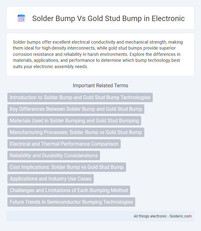
Introduction to Solder Bump and Gold Stud Bump Technologies
Solder bump technology involves depositing molten solder balls on semiconductor wafers to create electrical and mechanical connections in flip-chip packaging, providing excellent thermal and electrical conductivity. Gold stud bump technology uses ultrasonic bonding to form gold bumps on chip pads, offering superior bond reliability and resistance to corrosion without the need for flux. Both methods are critical in advanced microelectronics packaging, with solder bumps favoring cost efficiency and high-volume production while gold stud bumps excel in fine-pitch applications and harsh environments.
Key Differences Between Solder Bump and Gold Stud Bump
Solder bumps are composed primarily of tin-based alloys, providing excellent electrical conductivity and mechanical flexibility for microelectronic packaging, while gold stud bumps utilize pure gold, offering superior corrosion resistance and stronger wire bondability. Solder bumps typically require reflow processes for attachment, whereas gold stud bumps are formed through thermosonic bonding without additional heat, making them suitable for delicate substrates. Your choice between solder bump and gold stud bump depends on factors such as thermal budget, electrical performance, and environmental durability needed for your application.
Materials Used in Solder Bumping and Gold Stud Bumping
Solder bumping primarily utilizes alloys such as tin-lead (Sn-Pb), lead-free tin-silver-copper (Sn-Ag-Cu), or other lead-free solders optimized for reliability and electrical performance. Gold stud bumping involves the use of pure gold or gold-plated materials, which offer excellent conductivity, corrosion resistance, and bonding strength, especially in fine-pitch interconnect applications. The selection of materials directly impacts thermal stability, mechanical robustness, and overall interconnect quality in microelectronics packaging.
Manufacturing Processes: Solder Bump vs Gold Stud Bump
Solder bump manufacturing involves depositing molten solder onto a substrate through techniques like electroplating or printing, followed by reflow to form uniform bumps for flip-chip interconnections. Gold stud bump formation uses wire bonding to create gold protrusions directly on pads, which are then flattened to establish reliable connections without requiring additional flux or reflow. Your choice between these processes depends on factors such as thermal compatibility, mechanical reliability, and production complexity in semiconductor packaging.
Electrical and Thermal Performance Comparison
Solder bumps offer superior electrical conductivity with low resistance, making them ideal for high-frequency signal transmission, while gold stud bumps provide stable performance with excellent corrosion resistance but slightly higher resistance values. Thermal conductivity favors solder bumps as they effectively dissipate heat due to their metallurgical properties, enhancing device reliability under high power conditions. Your choice depends on balancing the need for electrical efficiency and thermal management in your specific semiconductor packaging application.
Reliability and Durability Considerations
Solder bumps exhibit excellent mechanical strength and thermal fatigue resistance, making them highly reliable for automated assembly processes with repeated thermal cycling. Gold stud bumps offer superior corrosion resistance and maintain electrical integrity under harsh environmental conditions, enhancing their durability in sensitive device applications. While solder bumps provide cost-effective, robust interconnections, gold stud bumps excel in long-term stability and low-contact resistance.
Cost Implications: Solder Bump vs Gold Stud Bump
Solder bumps generally offer lower material and processing costs compared to gold stud bumps, making them a cost-effective choice for large-scale semiconductor packaging. Gold stud bumps involve higher expense due to the premium price of gold and more complex fabrication processes, which can increase the overall manufacturing cost. Choosing solder bumps can significantly reduce production expenses without compromising reliability in many standard applications.
Applications and Industry Use Cases
Solder bumps are predominantly used in semiconductor packaging for high-volume manufacturing, offering excellent electrical conductivity and mechanical strength in applications like flip-chip assemblies and advanced integrated circuits. Gold stud bumps are favored in precision electronics and aerospace industries due to their superior corrosion resistance and reliable performance in harsh environments, making them ideal for microelectromechanical systems (MEMS) and high-reliability devices. Your choice between solder and gold stud bumps depends on the specific requirements of conductivity, durability, and environmental conditions in your industry applications.
Challenges and Limitations of Each Bumping Method
Solder bump technology faces challenges such as limited thermal and mechanical reliability under high-stress conditions, along with the risk of oxidation and flux residues affecting joint integrity. Gold stud bumping encounters limitations in cost due to the high price of gold, while also experiencing issues with wire deformation and difficulty in achieving consistent bump size for ultra-fine pitch applications. Both methods struggle with scaling for next-generation semiconductor packaging, demanding advancements in precision and material compatibility.
Future Trends in Semiconductor Bumping Technologies
Solder bump and gold stud bump technologies are evolving to meet the increasing demands for miniaturization and enhanced electrical performance in semiconductor packaging. Advanced materials like lead-free solder alloys and ultra-fine gold stud formations are driving improvements in reliability and thermal conductivity for next-generation devices. Your choice between these bumping techniques impacts device longevity and compatibility with emerging heterogeneous integration methods.
Solder bump vs Gold stud bump Infographic