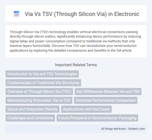
Through Silicon Via (TSV) technology enables vertical electrical connections passing directly through silicon wafers, significantly enhancing device performance by reducing signal delay and power consumption compared to traditional via methods that only traverse layers horizontally. Discover how TSV can revolutionize your semiconductor applications by exploring the detailed comparisons and benefits in the full article.
Comparison Table
| Aspect | VIA | TSV (Through Silicon Via) |
|---|---|---|
| Definition | Vertical electrical connection between metal layers in PCB or ICs | Vertical electrical connection passing completely through a silicon wafer or die |
| Material | Copper or plated metal in PCB/IC Layers | Copper-filled hole through silicon substrate |
| Application | Interconnect layers in PCBs and ICs for signal routing | 3D IC stacking, high-density interconnects, heterogeneous integration |
| Size | Micron scale (few microns diameter) | Typically 5-20 microns diameter, depth equals wafer thickness (100-800 microns) |
| Performance Impact | Enables layer-to-layer connectivity with moderate inductance/capacitance | Reduces signal delay and power by shortening interconnect length, improves bandwidth |
| Manufacturing Complexity | Standard PCB/IC fabrication processes | Advanced etching, filling, and wafer bonding technology required |
| Cost | Low to moderate cost, widely used in conventional electronics | Higher cost due to complex process and equipment |
| Key Benefits | Simple vertical interconnection, cost-effective for standard designs | Enables 3D integration, higher device density, enhanced electrical performance |
Introduction to Via and TSV Technologies
Via technology involves creating vertical electrical connections through insulating layers of semiconductor materials, enabling multi-layer circuit integration. Through Silicon Via (TSV) advances this concept by etching precise, high-aspect-ratio holes directly through silicon wafers, facilitating three-dimensional (3D) chip stacking with reduced interconnect lengths and enhanced performance. TSVs offer significant improvements in signal speed, power efficiency, and miniaturization compared to traditional vias, making them crucial for modern high-density integrated circuits and advanced packaging solutions.
Fundamentals of Traditional Via Structures
Traditional via structures in semiconductor devices involve vertical interconnect access that connects different metal layers on a chip, typically etched through dielectric materials and filled with conductive metals like copper. These vias serve as essential electrical pathways but are limited by aspect ratio constraints and increased parasitic capacitance, impacting signal integrity and performance in advanced nodes. Unlike TSVs, traditional vias do not pass through the silicon substrate itself, restricting their use to intra-layer or limited inter-layer connections within a single die.
Overview of Through Silicon Via (TSV)
Through Silicon Via (TSV) is an advanced 3D semiconductor packaging technology that vertically connects stacked silicon wafers through tiny, conductive holes etched directly into the silicon substrate. This method significantly enhances device performance by reducing signal path lengths, minimizing power consumption, and improving data transfer rates in integrated circuits. TSV is critical for your high-performance applications, enabling compact designs and improved reliability in memory and logic chip stacks.
Key Differences Between Via and TSV
Vias are traditional conductive pathways etched through printed circuit boards, typically used for inter-layer connections, while Through Silicon Vias (TSVs) enable vertical electrical connections directly through semiconductor wafers. TSVs offer significantly higher density, reduced signal delay, and improved performance in 3D integrated circuits compared to standard vias. Your choice between via and TSV technologies depends on design complexity, integration requirements, and performance goals in advanced microelectronics.
Manufacturing Processes: Via vs TSV
Via manufacturing involves creating vertical electrical connections through multiple layers of a printed circuit board using drilling and plating techniques, typically suitable for simpler and thinner substrates. TSV (Through Silicon Via) fabrication requires advanced semiconductor processes, including deep reactive-ion etching (DRIE), dielectric liner deposition, and copper filling, enabling high-density vertical interconnects within silicon wafers for 3D integrated circuits. Your choice between via and TSV depends on factors like layer count, electrical performance needs, and integration complexity in your device design.
Electrical Performance Comparison
Through Silicon Via (TSV) technology offers superior electrical performance compared to traditional vias by significantly reducing interconnect length and parasitic capacitance, resulting in lower signal delay and improved signal integrity. TSV enables higher bandwidth and lower power consumption due to its ability to create vertical interconnections through the silicon substrate, minimizing resistance and inductance effects. Your designs benefit from faster data transmission rates and enhanced signal reliability, making TSV ideal for advanced 3D integrated circuits and high-performance applications.
Space and Integration Density
TSVs (Through Silicon Vias) enable significantly higher integration density compared to traditional Vias by allowing vertical electrical connections through the silicon substrate, reducing interconnect length and improving signal integrity. TSV technology minimizes the footprint required for interconnects, optimizing space utilization in 3D integrated circuits and enabling more compact, high-performance semiconductor designs. This vertical integration reduces packaging complexity and enhances device miniaturization, critical for advanced applications like high-bandwidth memory and heterogeneous integration.
Applications and Use Cases
Via technology, commonly used in printed circuit boards, primarily facilitates electrical connections between different layers, supporting applications in consumer electronics and automotive systems. Through Silicon Via (TSV) enables vertical stacking of integrated circuits, significantly enhancing performance and reducing latency in high-density memory modules, 3D chip packaging, and advanced processors. TSV is integral to applications demanding high bandwidth and energy efficiency, such as artificial intelligence chips and mobile devices with compact form factors.
Challenges and Limitations
Through Silicon Via (TSV) technology faces challenges such as complex fabrication processes, high manufacturing costs, and thermal management issues due to the vertical interconnection through silicon substrates. Via structures without TSV often struggle with limited integration density and signal integrity problems, but they avoid the risks of wafer warping and mechanical stress common in TSV implementation. Both approaches encounter limitations in scalability and reliability, with TSVs demanding precise alignment and advanced materials to mitigate electrical resistance and thermal expansion mismatches.
Future Prospects in Semiconductor Packaging
TSVs (Through Silicon Vias) offer superior vertical interconnect density and electrical performance, making them a critical technology for 3D IC stacking and heterogeneous integration in semiconductor packaging. Vias, typically used in traditional PCB layers, provide simpler and cost-effective solutions but face limitations in scaling for ultra-high-density applications. The future of semiconductor packaging strongly favors TSV technology due to its potential for reduced signal delay, enhanced power efficiency, and enabling advanced chip architectures like high-bandwidth memory (HBM) and system-in-package (SiP) solutions.
Via vs TSV (Through Silicon Via) Infographic